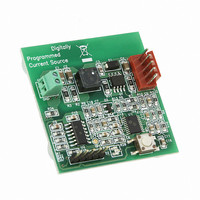
MCP1631RD-DCPC1 Microchip Technology, MCP1631RD-DCPC1 Datasheet - Page 68

MCP1631RD-DCPC1
Manufacturer Part Number
MCP1631RD-DCPC1
Description
REF DES BATT CHARG OR LED DRIVER
Manufacturer
Microchip Technology
Datasheets
1.PIC16F616T-ISL.pdf
(214 pages)
2.MCP1631VHVT-330EST.pdf
(34 pages)
3.MCP1631VHVT-330EST.pdf
(32 pages)
Specifications of MCP1631RD-DCPC1
Current - Output / Channel
700mA
Outputs And Type
1, Non-Isolated
Features
Firmware for Li-Ion, NiMH, and NiCd Battery Charger
Voltage - Input
3.5 ~ 16 V
Utilized Ic / Part
MCP1631HV, PIC16F616
Core Chip
MCP1631HV, PIC16F616
Topology
Parallel, Series
Output Current
1A
No. Of Outputs
1
Input Voltage
3.5V To 16V
Dimming Control Type
Analog
Kit Contents
Board
Lead Free Status / RoHS Status
Lead free / RoHS Compliant
Voltage - Output
-
Lead Free Status / Rohs Status
Lead free / RoHS Compliant
- PIC16F616T-ISL PDF datasheet
- MCP1631VHVT-330EST PDF datasheet #2
- MCP1631VHVT-330EST PDF datasheet #3
- Current page: 68 of 214
- Download datasheet (4Mb)
PIC16F610/616/16HV610/616
8.10
The SR latch module provides additional control of the
comparator outputs. The module consists of a single
SR latch and output multiplexers. The SR latch can be
set, reset or toggled by the comparator outputs. The SR
latch may also be set or reset, independent of
comparator output, by control bits in the SRCON0
control register. The SR latch output multiplexers select
whether the latch outputs or the comparator outputs are
directed to the I/O port logic for eventual output to a pin.
The SR latch also has a variable clock, which is
connected to the set input of the latch. The SRCLKEN
bit of SRCON0 enables the SR latch set clock. The
clock will periodically pulse the set input of the latch.
Control over the frequency of the SR latch set clock is
provided by the SRCS<1:0> bits of SRCON1 register.
8.10.1
The latch is a Set-Reset latch that does not depend on a
clock source. Each of the Set and Reset inputs are
active-high. Each latch input is connected to a
comparator output and a software controlled pulse
generator. The latch can be set by C1OUT or the PULSS
bit of the SRCON0 register. The latch can be reset by
C2OUT or the PULSR bit of the SRCON0 register. The
latch is reset-dominant, therefore, if both Set and Reset
FIGURE 8-8:
DS41288F-page 68
C1OUT (from comparator)
C1SEN
SYNCC2OUT (from comparator)
PULSS
C2REN
PULSR
Note 1:
Comparator SR Latch
LATCH OPERATION
2:
3:
If R = 1 and S = 1 simultaneously, Q = 0, Q = 1
Pulse generator causes a 1 T
Output shown for reference only. See I/O port pin block diagram for more detail.
Gen
Gen
Pulse
Pulse
SRCLKEN
SRCLK
(2)
(2)
SR LATCH SIMPLIFIED BLOCK DIAGRAM
OSC
pulse width.
SR
Latch
S
R
Q
Q
(1)
inputs are high the latch will go to the Reset state. Both
the PULSS and PULSR bits are self resetting which
means that a single write to either of the bits is all that is
necessary to complete a latch Set or Reset operation.
8.10.2
The SR<1:0> bits of the SRCON0 register control the
latch output multiplexers and determine four possible
output configurations. In these four configurations, the
CxOUT I/O port logic is connected to:
• C1OUT and C2OUT
• C1OUT and SR latch Q
• C2OUT and SR latch Q
• SR latch Q and Q
After any Reset, the default output configuration is the
unlatched C1OUT and C2OUT mode. This maintains
compatibility with devices that do not have the SR latch
feature.
The applicable TRIS bits of the corresponding ports
must be cleared to enable the port pin output drivers.
Additionally, the CxOE comparator output enable bits of
the CMxCON0 registers must be set in order to make the
comparator or latch outputs available on the output pins.
The latch configuration enable states are completely
independent of the enable states for the comparators.
SR0
SR1
LATCH OUTPUT
0
1
1
0
MUX
MUX
© 2009 Microchip Technology Inc.
C2OE
C1OE
C1OUT pin
C2OUT pin
(3)
(3)
Related parts for MCP1631RD-DCPC1
Image
Part Number
Description
Manufacturer
Datasheet
Request
R

Part Number:
Description:
REFERENCE DESIGN MCP1631HV
Manufacturer:
Microchip Technology
Datasheet:

Part Number:
Description:
REFERENCE DESIGN FOR MCP1631HV
Manufacturer:
Microchip Technology
Datasheet:

Part Number:
Description:
Manufacturer:
Microchip Technology Inc.
Datasheet:

Part Number:
Description:
Manufacturer:
Microchip Technology Inc.
Datasheet:

Part Number:
Description:
Manufacturer:
Microchip Technology Inc.
Datasheet:

Part Number:
Description:
Manufacturer:
Microchip Technology Inc.
Datasheet:

Part Number:
Description:
Manufacturer:
Microchip Technology Inc.
Datasheet:

Part Number:
Description:
Manufacturer:
Microchip Technology Inc.
Datasheet:

Part Number:
Description:
Manufacturer:
Microchip Technology Inc.
Datasheet:

Part Number:
Description:
Manufacturer:
Microchip Technology Inc.
Datasheet:


