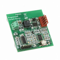
MCP1631RD-DCPC1 Microchip Technology, MCP1631RD-DCPC1 Datasheet - Page 143

MCP1631RD-DCPC1
Manufacturer Part Number
MCP1631RD-DCPC1
Description
REF DES BATT CHARG OR LED DRIVER
Manufacturer
Microchip Technology
Datasheets
1.PIC16F616T-ISL.pdf
(214 pages)
2.MCP1631VHVT-330EST.pdf
(34 pages)
3.MCP1631VHVT-330EST.pdf
(32 pages)
Specifications of MCP1631RD-DCPC1
Current - Output / Channel
700mA
Outputs And Type
1, Non-Isolated
Features
Firmware for Li-Ion, NiMH, and NiCd Battery Charger
Voltage - Input
3.5 ~ 16 V
Utilized Ic / Part
MCP1631HV, PIC16F616
Core Chip
MCP1631HV, PIC16F616
Topology
Parallel, Series
Output Current
1A
No. Of Outputs
1
Input Voltage
3.5V To 16V
Dimming Control Type
Analog
Kit Contents
Board
Lead Free Status / RoHS Status
Lead free / RoHS Compliant
Voltage - Output
-
Lead Free Status / Rohs Status
Lead free / RoHS Compliant
- PIC16F616T-ISL PDF datasheet
- MCP1631VHVT-330EST PDF datasheet #2
- MCP1631VHVT-330EST PDF datasheet #3
- Current page: 143 of 214
- Download datasheet (4Mb)
15.0
Absolute Maximum Ratings
Ambient temperature under bias..........................................................................................................-40° to +125°C
Storage temperature ........................................................................................................................ -65°C to +150°C
Voltage on V
Voltage on MCLR with respect to Vss ............................................................................................... -0.3V to +13.5V
Voltage on all other pins with respect to V
Total power dissipation
Maximum current out of V
Maximum current into V
Input clamp current, I
Output clamp current, I
Maximum output current sunk by any I/O pin.................................................................................................... 25 mA
Maximum output current sourced by any I/O pin .............................................................................................. 25 mA
Maximum current sunk by PORTA and PORTC (combined) ........................................................................... 90 mA
Maximum current sourced PORTA and PORTC (combined) ........................................................................... 90 mA
Note 1:
© 2009 Microchip Technology Inc.
† NOTICE: Stresses above those listed under “Absolute Maximum Ratings” may cause permanent damage to the
device. This is a stress rating only and functional operation of the device at those or any other conditions above those
indicated in the operation listings of this specification is not implied. Exposure above maximum rating conditions for
extended periods may affect device reliability.
ELECTRICAL SPECIFICATIONS
Power dissipation is calculated as follows: P
I
OL
DD
).
with respect to V
IK
(1)
OK
(V
DD
............................................................................................................................... 800 mW
I
SS
(Vo < 0 or Vo >V
< 0 or V
pin ......................................................................................................................... 95 mA
pin ...................................................................................................................... 95 mA
SS
I
> V
(†)
................................................................................................... -0.3V to +6.5V
DD
SS
)...............................................................................................................± 20 mA
DD
PIC16F610/616/16HV610/616
........................................................................... -0.3V to (V
).........................................................................................................± 20 mA
DIS
= V
DD
x {I
DD
– ∑ I
OH
} + ∑ {(V
DD
– V
OH
) x I
DS41288F-page 143
OH
} + ∑(V
DD
+ 0.3V)
O
l x
Related parts for MCP1631RD-DCPC1
Image
Part Number
Description
Manufacturer
Datasheet
Request
R

Part Number:
Description:
REFERENCE DESIGN MCP1631HV
Manufacturer:
Microchip Technology
Datasheet:

Part Number:
Description:
REFERENCE DESIGN FOR MCP1631HV
Manufacturer:
Microchip Technology
Datasheet:

Part Number:
Description:
Manufacturer:
Microchip Technology Inc.
Datasheet:

Part Number:
Description:
Manufacturer:
Microchip Technology Inc.
Datasheet:

Part Number:
Description:
Manufacturer:
Microchip Technology Inc.
Datasheet:

Part Number:
Description:
Manufacturer:
Microchip Technology Inc.
Datasheet:

Part Number:
Description:
Manufacturer:
Microchip Technology Inc.
Datasheet:

Part Number:
Description:
Manufacturer:
Microchip Technology Inc.
Datasheet:

Part Number:
Description:
Manufacturer:
Microchip Technology Inc.
Datasheet:

Part Number:
Description:
Manufacturer:
Microchip Technology Inc.
Datasheet:


