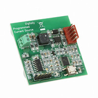
MCP1631RD-DCPC1 Microchip Technology, MCP1631RD-DCPC1 Datasheet - Page 59

MCP1631RD-DCPC1
Manufacturer Part Number
MCP1631RD-DCPC1
Description
REF DES BATT CHARG OR LED DRIVER
Manufacturer
Microchip Technology
Datasheets
1.PIC16F616T-ISL.pdf
(214 pages)
2.MCP1631VHVT-330EST.pdf
(34 pages)
3.MCP1631VHVT-330EST.pdf
(32 pages)
Specifications of MCP1631RD-DCPC1
Current - Output / Channel
700mA
Outputs And Type
1, Non-Isolated
Features
Firmware for Li-Ion, NiMH, and NiCd Battery Charger
Voltage - Input
3.5 ~ 16 V
Utilized Ic / Part
MCP1631HV, PIC16F616
Core Chip
MCP1631HV, PIC16F616
Topology
Parallel, Series
Output Current
1A
No. Of Outputs
1
Input Voltage
3.5V To 16V
Dimming Control Type
Analog
Kit Contents
Board
Lead Free Status / RoHS Status
Lead free / RoHS Compliant
Voltage - Output
-
Lead Free Status / Rohs Status
Lead free / RoHS Compliant
- PIC16F616T-ISL PDF datasheet
- MCP1631VHVT-330EST PDF datasheet #2
- MCP1631VHVT-330EST PDF datasheet #3
- Current page: 59 of 214
- Download datasheet (4Mb)
8.2
Each
Configuration register: CM1CON0 for Comparator C1
and CM2CON0 for Comparator C2. In addition,
Comparator C2 has a second control register,
CM2CON1, for controlling the interaction with Timer1 and
simultaneous reading of both comparator outputs.
The CM1CON0 and CM2CON0 registers (see Registers
8-1 and 8-2, respectively) contain the control and Status
bits for the following:
• Enable
• Input selection
• Reference selection
• Output selection
• Output polarity
8.2.1
Setting the CxON bit of the CMxCON0 register enables
the comparator for operation. Clearing the CxON bit
disables
consumption.
8.2.2
The CxCH<1:0> bits of the CMxCON0 register direct
one of four analog input pins to the comparator
inverting input.
8.2.3
Setting the CxR bit of the CMxCON0 register directs an
internal voltage reference or an analog input pin to the
non-inverting input of the comparator. See Section 8.11
“Comparator Voltage Reference” for more information
on the internal voltage reference module.
© 2009 Microchip Technology Inc.
Note:
comparator
Comparator Control
the
COMPARATOR ENABLE
COMPARATOR INPUT SELECTION
To use CxIN+ and CxIN- pins as analog
inputs, the appropriate bits must be set in
the ANSEL register and the corresponding
TRIS bits must also be set to disable the
output drivers.
COMPARATOR REFERENCE
SELECTION
comparator
has
a
for
separate
minimum
control
PIC16F610/616/16HV610/616
current
and
8.2.4
The output of the comparator can be monitored by
reading either the CxOUT bit of the CMxCON0 register
or the MCxOUT bit of the CM2CON1 register. In order
to make the output available for an external connection,
the following conditions must be true:
• CxOE bit of the CMxCON0 register must be set
• Corresponding TRIS bit must be cleared
• CxON bit of the CMxCON0 register must be set.
8.2.5
Inverting the output of the comparator is functionally
equivalent to swapping the comparator inputs. The
polarity of the comparator output can be inverted by
setting the CxPOL bit of the CMxCON0 register.
Clearing the CxPOL bit results in a non-inverted output.
Table 8-1 shows the output state versus input
conditions, including polarity control.
TABLE 8-1:
8.3
The comparator output is indeterminate for a period of
time after the change of an input source or the selection
of a new reference voltage. This period is referred to as
the response time. The response time of the
comparator differs from the settling time of the voltage
reference. Therefore, both of these times must be
considered when determining the total response time
to a comparator input change. See the Comparator and
Voltage Reference Specifications in Section 15.0
“Electrical Specifications” for more details.
Input Condition
CxV
CxV
CxV
CxV
Note 1: The CxOE bit overrides the PORT data
IN
IN
IN
IN
- > CxV
- < CxV
- > CxV
- < CxV
2: The internal output of the comparator is
Comparator Response Time
COMPARATOR OUTPUT SELECTION
COMPARATOR OUTPUT POLARITY
latch. Setting the CxON has no impact on
the port override.
latched with each instruction cycle.
Unless otherwise specified, external
outputs are not latched.
IN
IN
IN
IN
+
+
+
+
COMPARATOR OUTPUT
STATE VS. INPUT
CONDITIONS
CxPOL
0
0
1
1
DS41288F-page 59
CxOUT
0
1
1
0
Related parts for MCP1631RD-DCPC1
Image
Part Number
Description
Manufacturer
Datasheet
Request
R

Part Number:
Description:
REFERENCE DESIGN MCP1631HV
Manufacturer:
Microchip Technology
Datasheet:

Part Number:
Description:
REFERENCE DESIGN FOR MCP1631HV
Manufacturer:
Microchip Technology
Datasheet:

Part Number:
Description:
Manufacturer:
Microchip Technology Inc.
Datasheet:

Part Number:
Description:
Manufacturer:
Microchip Technology Inc.
Datasheet:

Part Number:
Description:
Manufacturer:
Microchip Technology Inc.
Datasheet:

Part Number:
Description:
Manufacturer:
Microchip Technology Inc.
Datasheet:

Part Number:
Description:
Manufacturer:
Microchip Technology Inc.
Datasheet:

Part Number:
Description:
Manufacturer:
Microchip Technology Inc.
Datasheet:

Part Number:
Description:
Manufacturer:
Microchip Technology Inc.
Datasheet:

Part Number:
Description:
Manufacturer:
Microchip Technology Inc.
Datasheet:


