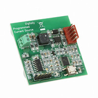
MCP1631RD-DCPC1 Microchip Technology, MCP1631RD-DCPC1 Datasheet - Page 45

MCP1631RD-DCPC1
Manufacturer Part Number
MCP1631RD-DCPC1
Description
REF DES BATT CHARG OR LED DRIVER
Manufacturer
Microchip Technology
Datasheets
1.PIC16F616T-ISL.pdf
(214 pages)
2.MCP1631VHVT-330EST.pdf
(34 pages)
3.MCP1631VHVT-330EST.pdf
(32 pages)
Specifications of MCP1631RD-DCPC1
Current - Output / Channel
700mA
Outputs And Type
1, Non-Isolated
Features
Firmware for Li-Ion, NiMH, and NiCd Battery Charger
Voltage - Input
3.5 ~ 16 V
Utilized Ic / Part
MCP1631HV, PIC16F616
Core Chip
MCP1631HV, PIC16F616
Topology
Parallel, Series
Output Current
1A
No. Of Outputs
1
Input Voltage
3.5V To 16V
Dimming Control Type
Analog
Kit Contents
Board
Lead Free Status / RoHS Status
Lead free / RoHS Compliant
Voltage - Output
-
Lead Free Status / Rohs Status
Lead free / RoHS Compliant
- PIC16F616T-ISL PDF datasheet
- MCP1631VHVT-330EST PDF datasheet #2
- MCP1631VHVT-330EST PDF datasheet #3
- Current page: 45 of 214
- Download datasheet (4Mb)
5.0
The Timer0 module is an 8-bit timer/counter with the
following features:
• 8-bit timer/counter register (TMR0)
• 8-bit prescaler (shared with Watchdog Timer)
• Programmable internal or external clock source
• Programmable external clock edge selection
• Interrupt on overflow
Figure 5-1 is a block diagram of the Timer0 module.
FIGURE 5-1:
© 2009 Microchip Technology Inc.
T0CKI
WDTE
pin
Note 1: T0SE, T0CS, PSA, PS<2:0> are bits in the OPTION register.
F
OSC
T0SE
TIMER0 MODULE
2: WDTE bit is in the Configuration Word register.
/4
Watchdog
Timer
BLOCK DIAGRAM OF THE TIMER0/WDT PRESCALER
T0CS
0
1
PSA
0
1
PIC16F610/616/16HV610/616
Prescaler
8-bit
8
PS<2:0>
5.1
When used as a timer, the Timer0 module can be used
as either an 8-bit timer or an 8-bit counter.
5.1.1
When used as a timer, the Timer0 module will
increment every instruction cycle (without prescaler).
Timer mode is selected by clearing the T0CS bit of the
OPTION register to ‘0’.
When TMR0 is written, the increment is inhibited for
two instruction cycles immediately following the write.
5.1.2
When used as a counter, the Timer0 module will
increment on every rising or falling edge of the T0CKI
pin. The incrementing edge is determined by the T0SE
bit of the OPTION register. Counter mode is selected by
setting the T0CS bit of the OPTION register to ‘1’.
Note:
3
Timer0 Operation
8-BIT TIMER MODE
The value written to the TMR0 register can
be adjusted, in order to account for the two
instruction cycle delay when TMR0 is
written.
8-BIT COUNTER MODE
PSA
PSA
1
0
1
0
Time-out
2 Tcy
Sync
WDT
Data Bus
DS41288F-page 45
Set Flag bit T0IF
8
TMR0
on Overflow
Related parts for MCP1631RD-DCPC1
Image
Part Number
Description
Manufacturer
Datasheet
Request
R

Part Number:
Description:
REFERENCE DESIGN MCP1631HV
Manufacturer:
Microchip Technology
Datasheet:

Part Number:
Description:
REFERENCE DESIGN FOR MCP1631HV
Manufacturer:
Microchip Technology
Datasheet:

Part Number:
Description:
Manufacturer:
Microchip Technology Inc.
Datasheet:

Part Number:
Description:
Manufacturer:
Microchip Technology Inc.
Datasheet:

Part Number:
Description:
Manufacturer:
Microchip Technology Inc.
Datasheet:

Part Number:
Description:
Manufacturer:
Microchip Technology Inc.
Datasheet:

Part Number:
Description:
Manufacturer:
Microchip Technology Inc.
Datasheet:

Part Number:
Description:
Manufacturer:
Microchip Technology Inc.
Datasheet:

Part Number:
Description:
Manufacturer:
Microchip Technology Inc.
Datasheet:

Part Number:
Description:
Manufacturer:
Microchip Technology Inc.
Datasheet:


