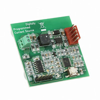
MCP1631RD-DCPC1 Microchip Technology, MCP1631RD-DCPC1 Datasheet - Page 33

MCP1631RD-DCPC1
Manufacturer Part Number
MCP1631RD-DCPC1
Description
REF DES BATT CHARG OR LED DRIVER
Manufacturer
Microchip Technology
Datasheets
1.PIC16F616T-ISL.pdf
(214 pages)
2.MCP1631VHVT-330EST.pdf
(34 pages)
3.MCP1631VHVT-330EST.pdf
(32 pages)
Specifications of MCP1631RD-DCPC1
Current - Output / Channel
700mA
Outputs And Type
1, Non-Isolated
Features
Firmware for Li-Ion, NiMH, and NiCd Battery Charger
Voltage - Input
3.5 ~ 16 V
Utilized Ic / Part
MCP1631HV, PIC16F616
Core Chip
MCP1631HV, PIC16F616
Topology
Parallel, Series
Output Current
1A
No. Of Outputs
1
Input Voltage
3.5V To 16V
Dimming Control Type
Analog
Kit Contents
Board
Lead Free Status / RoHS Status
Lead free / RoHS Compliant
Voltage - Output
-
Lead Free Status / Rohs Status
Lead free / RoHS Compliant
- PIC16F616T-ISL PDF datasheet
- MCP1631VHVT-330EST PDF datasheet #2
- MCP1631VHVT-330EST PDF datasheet #3
- Current page: 33 of 214
- Download datasheet (4Mb)
4.0
There are as many as eleven general purpose I/O pins
and an input pin available. Depending on which
peripherals are enabled, some or all of the pins may not
be available as general purpose I/O. In general, when a
peripheral is enabled, the associated pin may not be
used as a general purpose I/O pin.
4.1
PORTA is a 6-bit wide, bidirectional port. The
corresponding
(Register 4-2). Setting a TRISA bit (= 1) will make the
corresponding PORTA pin an input (i.e., disable the
output driver). Clearing a TRISA bit (= 0) will make the
corresponding PORTA pin an output (i.e., enables output
driver and puts the contents of the output latch on the
selected pin). The exception is RA3, which is input only
and its TRIS bit will always read as ‘1’. Example 4-1
shows how to initialize PORTA.
Reading the PORTA register (Register 4-1) reads the
status of the pins, whereas writing to it will write to the
PORT latch. All write operations are read-modify-write
operations. Therefore, a write to a port implies that the
REGISTER 4-1:
REGISTER 4-2:
© 2009 Microchip Technology Inc.
bit 7
Legend:
R = Readable bit
-n = Value at POR
bit 7-6
bit 5-0
bit 7
Legend:
R = Readable bit
-n = Value at POR
bit 7-6
bit 5-0
Note 1:
U-0
U-0
—
—
2:
I/O PORTS
PORTA and the TRISA Registers
TRISA<3> always reads ‘1’.
TRISA<5:4> always reads ‘1’ in XT, HS and LP Oscillator modes.
data
Unimplemented: Read as ‘0’
RA<5:0>: PORTA I/O Pin bit
1 = PORTA pin is > V
0 = PORTA pin is < V
Unimplemented: Read as ‘0’
TRISA<5:0>: PORTA Tri-State Control bit
1 = PORTA pin configured as an input (tri-stated)
0 = PORTA pin configured as an output
U-0
U-0
—
—
PORTA: PORTA REGISTER
TRISA: PORTA TRI-STATE REGISTER
direction
W = Writable bit
‘1’ = Bit is set
W = Writable bit
‘1’ = Bit is set
register
TRISA5
R/W-x
R/W-1
IH
IL
RA5
PIC16F610/616/16HV610/616
is
TRISA
TRISA4
R/W-0
R/W-1
RA4
U = Unimplemented bit, read as ‘0’
U = Unimplemented bit, read as ‘0’
‘0’ = Bit is cleared
‘0’ = Bit is cleared
TRISA3
port pins are read, this value is modified and then
written to the PORT data latch. RA3 reads ‘0’ when
MCLRE = 1.
The TRISA register controls the direction of the
PORTA pins, even when they are being used as
analog inputs. The user must ensure the bits in the
TRISA register are maintained set when using them as
analog inputs. I/O pins configured as analog input
always read ‘0’.
EXAMPLE 4-1:
RA3
R-x
R-1
BCF
CLRF
BSF
CLRF
MOVLW 0Ch
MOVWF TRISA
BCF
Note:
STATUS,RP0
PORTA
STATUS,RP0
ANSEL
STATUS,RP0
The ANSEL register must be initialized to
configure an analog channel as a digital
input. Pins configured as analog inputs will
read ‘0’ and cannot generate an interrupt.
TRISA2
R/W-0
R/W-1
RA2
INITIALIZING PORTA
x = Bit is unknown
x = Bit is unknown
;Bank 0
;Init PORTA
;Bank 1
;digital I/O
;Set RA<3:2> as inputs
;and set RA<5:4,1:0>
;as outputs
;Bank 0
TRISA1
R/W-0
R/W-1
RA1
DS41288F-page 33
TRISA0
R/W-0
R/W-1
RA0
bit 0
bit 0
Related parts for MCP1631RD-DCPC1
Image
Part Number
Description
Manufacturer
Datasheet
Request
R

Part Number:
Description:
REFERENCE DESIGN MCP1631HV
Manufacturer:
Microchip Technology
Datasheet:

Part Number:
Description:
REFERENCE DESIGN FOR MCP1631HV
Manufacturer:
Microchip Technology
Datasheet:

Part Number:
Description:
Manufacturer:
Microchip Technology Inc.
Datasheet:

Part Number:
Description:
Manufacturer:
Microchip Technology Inc.
Datasheet:

Part Number:
Description:
Manufacturer:
Microchip Technology Inc.
Datasheet:

Part Number:
Description:
Manufacturer:
Microchip Technology Inc.
Datasheet:

Part Number:
Description:
Manufacturer:
Microchip Technology Inc.
Datasheet:

Part Number:
Description:
Manufacturer:
Microchip Technology Inc.
Datasheet:

Part Number:
Description:
Manufacturer:
Microchip Technology Inc.
Datasheet:

Part Number:
Description:
Manufacturer:
Microchip Technology Inc.
Datasheet:


