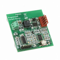
MCP1631RD-DCPC1 Microchip Technology, MCP1631RD-DCPC1 Datasheet - Page 164

MCP1631RD-DCPC1
Manufacturer Part Number
MCP1631RD-DCPC1
Description
REF DES BATT CHARG OR LED DRIVER
Manufacturer
Microchip Technology
Datasheets
1.PIC16F616T-ISL.pdf
(214 pages)
2.MCP1631VHVT-330EST.pdf
(34 pages)
3.MCP1631VHVT-330EST.pdf
(32 pages)
Specifications of MCP1631RD-DCPC1
Current - Output / Channel
700mA
Outputs And Type
1, Non-Isolated
Features
Firmware for Li-Ion, NiMH, and NiCd Battery Charger
Voltage - Input
3.5 ~ 16 V
Utilized Ic / Part
MCP1631HV, PIC16F616
Core Chip
MCP1631HV, PIC16F616
Topology
Parallel, Series
Output Current
1A
No. Of Outputs
1
Input Voltage
3.5V To 16V
Dimming Control Type
Analog
Kit Contents
Board
Lead Free Status / RoHS Status
Lead free / RoHS Compliant
Voltage - Output
-
Lead Free Status / Rohs Status
Lead free / RoHS Compliant
- PIC16F616T-ISL PDF datasheet
- MCP1631VHVT-330EST PDF datasheet #2
- MCP1631VHVT-330EST PDF datasheet #3
- Current page: 164 of 214
- Download datasheet (4Mb)
PIC16F610/616/16HV610/616
TABLE 15-7:
TABLE 15-8:
TABLE 15-9:
DS41288F-page 164
Standard Operating Conditions (unless otherwise stated)
Operating Temperature
CM01
CM02
CM03* C
CM04* T
CM05* T
CM06* V
Note 1:
Standard Operating Conditions (unless otherwise stated)
Operating temperature
CV01
CV02
CV03
CV04
VR Voltage Reference Specifications
VR01
VR02
VR03*
Param
Param
Param
No.
No.
No.
2:
*
† Data in “Typ” column is at 5V, 25°C unless otherwise stated. These parameters are for design guidance
*
V
V
C
C
C
C
Note 1:
VP6
V1P2
T
RT
OS
MC
CM
HYS
STABLE
MRR
Symbol
LSB
ACC
R
ST
These parameters are characterized but not tested.
only and are not tested.
Response time is measured with one comparator input at (V
The other input is at (V
Input offset voltage is measured with one comparator input at (V
Sym
These parameters are characterized but not tested.
Sym
2
OUT
CO
OUT
2:
3:
V Comparator Mode Change to Output Valid
† Data in “Typ” column is at 5V, 25°C unless otherwise stated. These parameters are for design
COMPARATOR SPECIFICATIONS
COMPARATOR VOLTAGE REFERENCE (CV
VOLTAGE REFERENCE SPECIFICATIONS
Step Size
Absolute Accuracy
Unit Resistor Value (R)
Settling Time
Input Offset Voltage
Input Common Mode Voltage
Common Mode Rejection Ratio
Response Time
Input Hysteresis Voltage
guidance only and are not tested.
Settling time measured while VRR = 1 and VR<3:0> transitions from ‘0000’ to ‘1111’.
See Section 8.11 “Comparator Voltage Reference” for more information.
Absolute Accuracy when CV
VP6 voltage output
V1P2 voltage output
Settling Time
-40°C ≤ T
-40°C ≤ T
Characteristics
(2)
Characteristics
(1)
Characteristics
DD
(1)
A
A
-1.5)/2.
(3)
≤ +125°C
≤ +125°C
(2)
REF
output is ≤ (V
Standard Operating Conditions (unless otherwise stated)
Operating temperature
Falling
Rising
Min
0.50
1.05
Min
—
—
—
—
—
—
—
V
V
Typ†
DD
DD
2k
Min
+55
—
—
—
1.20
DD
Typ
0.6
—
—
—
—
—
10
0
/24
/32
-1.5).
REF
DD
Typ†
± 5.0
) SPECIFICATIONS
± 1/2
± 1/2
150
200
- 1.5)/2 - 100 mV to (V
Max
45
—
—
—
10
—
—
—
DD
1.35
Max
0.7
—
- 1.5V)/2.
V
-40°C ≤ T
DD
Units
1000
LSb
LSb
Max
± 10
600
μs
10
60
Ω
—
V
V
Units
– 1.5
© 2009 Microchip Technology Inc.
μs
V
V
Low Range (VRR = 1)
High Range (VRR = 0)
Low Range (VRR = 1)
High Range (VRR = 0)
A
Units
≤ +125°C
mV
mV
dB
ns
ns
μs
V
DD
Comments
- 1.5)/2 + 20 mV.
Comments
Comments
Related parts for MCP1631RD-DCPC1
Image
Part Number
Description
Manufacturer
Datasheet
Request
R

Part Number:
Description:
REFERENCE DESIGN MCP1631HV
Manufacturer:
Microchip Technology
Datasheet:

Part Number:
Description:
REFERENCE DESIGN FOR MCP1631HV
Manufacturer:
Microchip Technology
Datasheet:

Part Number:
Description:
Manufacturer:
Microchip Technology Inc.
Datasheet:

Part Number:
Description:
Manufacturer:
Microchip Technology Inc.
Datasheet:

Part Number:
Description:
Manufacturer:
Microchip Technology Inc.
Datasheet:

Part Number:
Description:
Manufacturer:
Microchip Technology Inc.
Datasheet:

Part Number:
Description:
Manufacturer:
Microchip Technology Inc.
Datasheet:

Part Number:
Description:
Manufacturer:
Microchip Technology Inc.
Datasheet:

Part Number:
Description:
Manufacturer:
Microchip Technology Inc.
Datasheet:

Part Number:
Description:
Manufacturer:
Microchip Technology Inc.
Datasheet:


