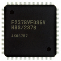
DF61657CN35FTV Renesas Electronics America, DF61657CN35FTV Datasheet - Page 815

DF61657CN35FTV
Manufacturer Part Number
DF61657CN35FTV
Description
IC H8SX/1657 MCU FLASH 120TQFP
Manufacturer
Renesas Electronics America
Series
H8® H8SX/1600r
Datasheet
1.DF61656N35FTV.pdf
(894 pages)
Specifications of DF61657CN35FTV
Core Processor
H8SX
Core Size
32-Bit
Speed
35MHz
Connectivity
SCI, SmartCard
Peripherals
DMA, PWM, WDT
Number Of I /o
82
Program Memory Size
768KB (768K x 8)
Program Memory Type
FLASH
Ram Size
24K x 8
Voltage - Supply (vcc/vdd)
3 V ~ 3.6 V
Data Converters
A/D 8x10b; D/A 2x8b
Oscillator Type
Internal
Operating Temperature
-20°C ~ 75°C
Package / Case
120-TQFP, 120-VQFP
For Use With
3DK1657 - DEV EVAL KIT FOR H8SX/1657
Lead Free Status / RoHS Status
Lead free / RoHS Compliant
Eeprom Size
-
Available stocks
Company
Part Number
Manufacturer
Quantity
Price
Company:
Part Number:
DF61657CN35FTV
Manufacturer:
RENESAS
Quantity:
101
Company:
Part Number:
DF61657CN35FTV
Manufacturer:
Renesas Electronics America
Quantity:
10 000
- Current page: 815 of 894
- Download datasheet (5Mb)
Note: *
Register Name
Timer general register A_3
Timer general register B_3
Timer general register C_3
Timer general register D_3
When the same output trigger is specified for pulse output groups 2 and 3 by the PCR
setting, the NDRH address is H'FFF7C. When different output triggers are specified, the
NDRH addresses for pulse output groups 2 and 3 are H'FFF7E and H'FFF7C,
respectively. Similarly, When the same output trigger is specified for pulse output groups
0 and 1 by the PCR setting, the NDRL address is H'FFF7D. When different output
triggers are specified, the NDRL addresses for pulse output groups 0 and 1 are H'FFF7F
and H'FFF7D, respectively.
Abbreviation
TGRA_3
TGRB_3
TGRC_3
TGRD_3
Number
of Bits
16
16
16
16
H'FFFF8
H'FFFFA
Address
H'FFFFC
H'FFFFE
Rev. 2.00 Jun. 28, 2007 Page 789 of 864
Module
TPU_3
TPU_3
TPU_3
TPU_3
Section 21 List of Registers
Data
Width
16
16
16
16
REJ09B0341-0200
Access
Cycles
(Read/Write)
2Pφ/2Pφ
2Pφ/2Pφ
2Pφ/2Pφ
2Pφ/2Pφ
Related parts for DF61657CN35FTV
Image
Part Number
Description
Manufacturer
Datasheet
Request
R

Part Number:
Description:
KIT STARTER FOR M16C/29
Manufacturer:
Renesas Electronics America
Datasheet:

Part Number:
Description:
KIT STARTER FOR R8C/2D
Manufacturer:
Renesas Electronics America
Datasheet:

Part Number:
Description:
R0K33062P STARTER KIT
Manufacturer:
Renesas Electronics America
Datasheet:

Part Number:
Description:
KIT STARTER FOR R8C/23 E8A
Manufacturer:
Renesas Electronics America
Datasheet:

Part Number:
Description:
KIT STARTER FOR R8C/25
Manufacturer:
Renesas Electronics America
Datasheet:

Part Number:
Description:
KIT STARTER H8S2456 SHARPE DSPLY
Manufacturer:
Renesas Electronics America
Datasheet:

Part Number:
Description:
KIT STARTER FOR R8C38C
Manufacturer:
Renesas Electronics America
Datasheet:

Part Number:
Description:
KIT STARTER FOR R8C35C
Manufacturer:
Renesas Electronics America
Datasheet:

Part Number:
Description:
KIT STARTER FOR R8CL3AC+LCD APPS
Manufacturer:
Renesas Electronics America
Datasheet:

Part Number:
Description:
KIT STARTER FOR RX610
Manufacturer:
Renesas Electronics America
Datasheet:

Part Number:
Description:
KIT STARTER FOR R32C/118
Manufacturer:
Renesas Electronics America
Datasheet:

Part Number:
Description:
KIT DEV RSK-R8C/26-29
Manufacturer:
Renesas Electronics America
Datasheet:

Part Number:
Description:
KIT STARTER FOR SH7124
Manufacturer:
Renesas Electronics America
Datasheet:

Part Number:
Description:
KIT STARTER FOR H8SX/1622
Manufacturer:
Renesas Electronics America
Datasheet:

Part Number:
Description:
KIT DEV FOR SH7203
Manufacturer:
Renesas Electronics America
Datasheet:


