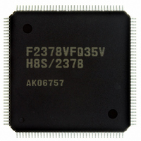
DF61657CN35FTV Renesas Electronics America, DF61657CN35FTV Datasheet - Page 791

DF61657CN35FTV
Manufacturer Part Number
DF61657CN35FTV
Description
IC H8SX/1657 MCU FLASH 120TQFP
Manufacturer
Renesas Electronics America
Series
H8® H8SX/1600r
Datasheet
1.DF61656N35FTV.pdf
(894 pages)
Specifications of DF61657CN35FTV
Core Processor
H8SX
Core Size
32-Bit
Speed
35MHz
Connectivity
SCI, SmartCard
Peripherals
DMA, PWM, WDT
Number Of I /o
82
Program Memory Size
768KB (768K x 8)
Program Memory Type
FLASH
Ram Size
24K x 8
Voltage - Supply (vcc/vdd)
3 V ~ 3.6 V
Data Converters
A/D 8x10b; D/A 2x8b
Oscillator Type
Internal
Operating Temperature
-20°C ~ 75°C
Package / Case
120-TQFP, 120-VQFP
For Use With
3DK1657 - DEV EVAL KIT FOR H8SX/1657
Lead Free Status / RoHS Status
Lead free / RoHS Compliant
Eeprom Size
-
Available stocks
Company
Part Number
Manufacturer
Quantity
Price
Company:
Part Number:
DF61657CN35FTV
Manufacturer:
RENESAS
Quantity:
101
Company:
Part Number:
DF61657CN35FTV
Manufacturer:
Renesas Electronics America
Quantity:
10 000
- Current page: 791 of 894
- Download datasheet (5Mb)
20.3
When bits ICK2 to ICK0, PCK2 to PCK0, and BCK2 to BCK0 in SCKCR are set, the main clock
frequency changes at the end of the bus cycle. The CPU and bus masters operate on the operating
clock specified by bits ICK2 to ICK0. The peripheral modules operate on the operating clock
specified by bits PCK2 to PCK0. The external bus clock operates on the operating clock specified
by bits BCK2 to BCK0. Even if the frequencies specified by bits PCK2 to PCK0 and BCK2 to
BCK0 are higher than the frequency specified by bits ICK2 to ICK0, the specified values are not
reflected in the peripheral module and external bus clocks. The peripheral module and external bus
clocks are restricted to the operating clock specified by bits ICK2 to ICK0.
20.4
Module stop function can be set for individual on-chip peripheral modules.
When the corresponding MSTP bit in MSTPCRA, MSTPCRB, or MSTPCRC is set to 1, module
operation stops at the end of the bus cycle and a transition is made to the module stop state. The
CPU continues operating independently.
When the corresponding MSTP bit is cleared to 0, the module stop state is cleared and the module
starts operating at the end of the bus cycle. In the module stop state, the internal states of modules
other than the SCI are retained.
After the reset state is cleared, all modules other than the DMAC, DTC, and on-chip RAM are in
the module stop state.
The registers of the module for which the module stop state is selected cannot be read from or
written to.
20.5
20.5.1
When the SLEEP instruction is executed when the SSBY bit in SBYCR is 0, the CPU enters sleep
mode. In sleep mode, CPU operation stops but the contents of the CPU's internal registers are
retained. Other peripheral functions do not stop.
Multi-Clock Function
Module Stop Function
Sleep Mode
Transition to Sleep Mode
Rev. 2.00 Jun. 28, 2007 Page 765 of 864
Section 20 Power-Down Modes
REJ09B0341-0200
Related parts for DF61657CN35FTV
Image
Part Number
Description
Manufacturer
Datasheet
Request
R

Part Number:
Description:
KIT STARTER FOR M16C/29
Manufacturer:
Renesas Electronics America
Datasheet:

Part Number:
Description:
KIT STARTER FOR R8C/2D
Manufacturer:
Renesas Electronics America
Datasheet:

Part Number:
Description:
R0K33062P STARTER KIT
Manufacturer:
Renesas Electronics America
Datasheet:

Part Number:
Description:
KIT STARTER FOR R8C/23 E8A
Manufacturer:
Renesas Electronics America
Datasheet:

Part Number:
Description:
KIT STARTER FOR R8C/25
Manufacturer:
Renesas Electronics America
Datasheet:

Part Number:
Description:
KIT STARTER H8S2456 SHARPE DSPLY
Manufacturer:
Renesas Electronics America
Datasheet:

Part Number:
Description:
KIT STARTER FOR R8C38C
Manufacturer:
Renesas Electronics America
Datasheet:

Part Number:
Description:
KIT STARTER FOR R8C35C
Manufacturer:
Renesas Electronics America
Datasheet:

Part Number:
Description:
KIT STARTER FOR R8CL3AC+LCD APPS
Manufacturer:
Renesas Electronics America
Datasheet:

Part Number:
Description:
KIT STARTER FOR RX610
Manufacturer:
Renesas Electronics America
Datasheet:

Part Number:
Description:
KIT STARTER FOR R32C/118
Manufacturer:
Renesas Electronics America
Datasheet:

Part Number:
Description:
KIT DEV RSK-R8C/26-29
Manufacturer:
Renesas Electronics America
Datasheet:

Part Number:
Description:
KIT STARTER FOR SH7124
Manufacturer:
Renesas Electronics America
Datasheet:

Part Number:
Description:
KIT STARTER FOR H8SX/1622
Manufacturer:
Renesas Electronics America
Datasheet:

Part Number:
Description:
KIT DEV FOR SH7203
Manufacturer:
Renesas Electronics America
Datasheet:


