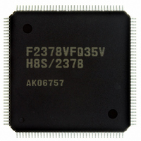
DF61657CN35FTV Renesas Electronics America, DF61657CN35FTV Datasheet - Page 658

DF61657CN35FTV
Manufacturer Part Number
DF61657CN35FTV
Description
IC H8SX/1657 MCU FLASH 120TQFP
Manufacturer
Renesas Electronics America
Series
H8® H8SX/1600r
Datasheet
1.DF61656N35FTV.pdf
(894 pages)
Specifications of DF61657CN35FTV
Core Processor
H8SX
Core Size
32-Bit
Speed
35MHz
Connectivity
SCI, SmartCard
Peripherals
DMA, PWM, WDT
Number Of I /o
82
Program Memory Size
768KB (768K x 8)
Program Memory Type
FLASH
Ram Size
24K x 8
Voltage - Supply (vcc/vdd)
3 V ~ 3.6 V
Data Converters
A/D 8x10b; D/A 2x8b
Oscillator Type
Internal
Operating Temperature
-20°C ~ 75°C
Package / Case
120-TQFP, 120-VQFP
For Use With
3DK1657 - DEV EVAL KIT FOR H8SX/1657
Lead Free Status / RoHS Status
Lead free / RoHS Compliant
Eeprom Size
-
Available stocks
Company
Part Number
Manufacturer
Quantity
Price
Company:
Part Number:
DF61657CN35FTV
Manufacturer:
RENESAS
Quantity:
101
Company:
Part Number:
DF61657CN35FTV
Manufacturer:
Renesas Electronics America
Quantity:
10 000
- Current page: 658 of 894
- Download datasheet (5Mb)
Section 15 A/D Converter
[Legend]
X: Don't care
Note:
15.4
The A/D converter operates by successive approximation with 10-bit resolution. It has two
operating modes: single mode and scan mode. When changing the operating mode or analog input
channel, to prevent incorrect operation, first clear the ADST bit in ADCSR to 0 to halt A/D
conversion. The ADST bit can be set to 1 at the same time as the operating mode or analog input
channel is changed.
15.4.1
In single mode, A/D conversion is to be performed only once on the analog input of the specified
single channel.
1. A/D conversion for the selected channel is started when the ADST bit in ADCSR is set to 1 by
2. When A/D conversion is completed, the A/D conversion result is transferred to the
3. When A/D conversion is completed, the ADF bit in ADCSR is set to 1. If the ADIE bit is set
4. The ADST bit remains set to 1 during A/D conversion, and is automatically cleared to 0 when
Rev. 2.00 Jun. 28, 2007 Page 632 of 864
REJ09B0341-0200
Bit
1, 0
software or an external trigger input.
corresponding A/D data register of the channel.
to 1 at this time, an ADI interrupt request is generated.
A/D conversion ends. The A/D converter enters wait state. If the ADST bit is cleared to 0
during A/D conversion, A/D conversion stops and the A/D converter enters wait state.
*
Bit Name
Operation
Single Mode
To set A/D conversion to start by the ADTRG pin, the DDR bit and ICR bit for the
corresponding pin should be set to 0 and 1, respectively. For details, refer to section 9,
I/O Ports.
Initial
Value
All 0
R/W
R
Description
Reserved
These are read-only bits and cannot be modified.
Related parts for DF61657CN35FTV
Image
Part Number
Description
Manufacturer
Datasheet
Request
R

Part Number:
Description:
KIT STARTER FOR M16C/29
Manufacturer:
Renesas Electronics America
Datasheet:

Part Number:
Description:
KIT STARTER FOR R8C/2D
Manufacturer:
Renesas Electronics America
Datasheet:

Part Number:
Description:
R0K33062P STARTER KIT
Manufacturer:
Renesas Electronics America
Datasheet:

Part Number:
Description:
KIT STARTER FOR R8C/23 E8A
Manufacturer:
Renesas Electronics America
Datasheet:

Part Number:
Description:
KIT STARTER FOR R8C/25
Manufacturer:
Renesas Electronics America
Datasheet:

Part Number:
Description:
KIT STARTER H8S2456 SHARPE DSPLY
Manufacturer:
Renesas Electronics America
Datasheet:

Part Number:
Description:
KIT STARTER FOR R8C38C
Manufacturer:
Renesas Electronics America
Datasheet:

Part Number:
Description:
KIT STARTER FOR R8C35C
Manufacturer:
Renesas Electronics America
Datasheet:

Part Number:
Description:
KIT STARTER FOR R8CL3AC+LCD APPS
Manufacturer:
Renesas Electronics America
Datasheet:

Part Number:
Description:
KIT STARTER FOR RX610
Manufacturer:
Renesas Electronics America
Datasheet:

Part Number:
Description:
KIT STARTER FOR R32C/118
Manufacturer:
Renesas Electronics America
Datasheet:

Part Number:
Description:
KIT DEV RSK-R8C/26-29
Manufacturer:
Renesas Electronics America
Datasheet:

Part Number:
Description:
KIT STARTER FOR SH7124
Manufacturer:
Renesas Electronics America
Datasheet:

Part Number:
Description:
KIT STARTER FOR H8SX/1622
Manufacturer:
Renesas Electronics America
Datasheet:

Part Number:
Description:
KIT DEV FOR SH7203
Manufacturer:
Renesas Electronics America
Datasheet:


