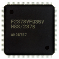
DF61657CN35FTV Renesas Electronics America, DF61657CN35FTV Datasheet - Page 438

DF61657CN35FTV
Manufacturer Part Number
DF61657CN35FTV
Description
IC H8SX/1657 MCU FLASH 120TQFP
Manufacturer
Renesas Electronics America
Series
H8® H8SX/1600r
Datasheet
1.DF61656N35FTV.pdf
(894 pages)
Specifications of DF61657CN35FTV
Core Processor
H8SX
Core Size
32-Bit
Speed
35MHz
Connectivity
SCI, SmartCard
Peripherals
DMA, PWM, WDT
Number Of I /o
82
Program Memory Size
768KB (768K x 8)
Program Memory Type
FLASH
Ram Size
24K x 8
Voltage - Supply (vcc/vdd)
3 V ~ 3.6 V
Data Converters
A/D 8x10b; D/A 2x8b
Oscillator Type
Internal
Operating Temperature
-20°C ~ 75°C
Package / Case
120-TQFP, 120-VQFP
For Use With
3DK1657 - DEV EVAL KIT FOR H8SX/1657
Lead Free Status / RoHS Status
Lead free / RoHS Compliant
Eeprom Size
-
Available stocks
Company
Part Number
Manufacturer
Quantity
Price
Company:
Part Number:
DF61657CN35FTV
Manufacturer:
RENESAS
Quantity:
101
Company:
Part Number:
DF61657CN35FTV
Manufacturer:
Renesas Electronics America
Quantity:
10 000
- Current page: 438 of 894
- Download datasheet (5Mb)
Section 10 16-Bit Timer Pulse Unit (TPU)
10.3.1
TCR controls the TCNT operation for each channel. The TPU has a total of six TCR registers, one
for each channel. TCR register settings should be made only while TCNT operation is stopped.
Rev. 2.00 Jun. 28, 2007 Page 412 of 864
REJ09B0341-0200
Bit
7
6
5
4
3
2
1
0
Bit
Bit Name
Initial Value
R/W
Bit Name
CCLR2
CCLR1
CCLR0
CKEG1
CKEG0
TPSC2
TPSC1
TPSC0
Timer Control Register (TCR)
CCLR2
R/W
7
0
Initial
Value
0
0
0
0
0
0
0
0
CCLR1
R/W
6
0
R/W
R/W
R/W
R/W
R/W
R/W
R/W
R/W
R/W
CCLR0
R/W
5
0
Description
Counter Clear 2 to 0
These bits select the TCNT counter clearing source. For
details, see tables 10.3 and 10.4.
Clock Edge 1 and 0
These bits select the input clock edge. For details, see
table 10.5. When the input clock is counted using both
edges, the input clock period is halved (e.g. Pφ/4 both
edges = Pφ/2 rising edge). If phase counting mode is
used on channels 1, 2, 4, and 5, this setting is ignored
and the phase counting mode setting has priority. Internal
clock edge selection is valid when the input clock is Pφ/4
or slower. This setting is ignored if the input clock is Pφ/1,
or when overflow/underflow of another channel is
selected.
Timer Prescaler 2 to 0
These bits select the TCNT counter clock. The clock
source can be selected independently for each channel.
For details, see tables 10.6 to 10.11. To select the
external clock as the clock source, the DDR bit and ICR
bit for the corresponding pin should be set to 0 and 1,
respectively. For details, see section 9, I/O Ports.
CKEG1
R/W
4
0
CKEG0
R/W
3
0
TPSC2
R/W
2
0
TPSC1
R/W
1
0
TPSC0
R/W
0
0
Related parts for DF61657CN35FTV
Image
Part Number
Description
Manufacturer
Datasheet
Request
R

Part Number:
Description:
KIT STARTER FOR M16C/29
Manufacturer:
Renesas Electronics America
Datasheet:

Part Number:
Description:
KIT STARTER FOR R8C/2D
Manufacturer:
Renesas Electronics America
Datasheet:

Part Number:
Description:
R0K33062P STARTER KIT
Manufacturer:
Renesas Electronics America
Datasheet:

Part Number:
Description:
KIT STARTER FOR R8C/23 E8A
Manufacturer:
Renesas Electronics America
Datasheet:

Part Number:
Description:
KIT STARTER FOR R8C/25
Manufacturer:
Renesas Electronics America
Datasheet:

Part Number:
Description:
KIT STARTER H8S2456 SHARPE DSPLY
Manufacturer:
Renesas Electronics America
Datasheet:

Part Number:
Description:
KIT STARTER FOR R8C38C
Manufacturer:
Renesas Electronics America
Datasheet:

Part Number:
Description:
KIT STARTER FOR R8C35C
Manufacturer:
Renesas Electronics America
Datasheet:

Part Number:
Description:
KIT STARTER FOR R8CL3AC+LCD APPS
Manufacturer:
Renesas Electronics America
Datasheet:

Part Number:
Description:
KIT STARTER FOR RX610
Manufacturer:
Renesas Electronics America
Datasheet:

Part Number:
Description:
KIT STARTER FOR R32C/118
Manufacturer:
Renesas Electronics America
Datasheet:

Part Number:
Description:
KIT DEV RSK-R8C/26-29
Manufacturer:
Renesas Electronics America
Datasheet:

Part Number:
Description:
KIT STARTER FOR SH7124
Manufacturer:
Renesas Electronics America
Datasheet:

Part Number:
Description:
KIT STARTER FOR H8SX/1622
Manufacturer:
Renesas Electronics America
Datasheet:

Part Number:
Description:
KIT DEV FOR SH7203
Manufacturer:
Renesas Electronics America
Datasheet:


