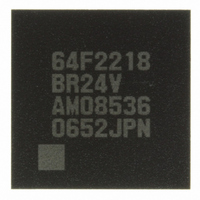
DF2218BR24V Renesas Electronics America, DF2218BR24V Datasheet - Page 665

DF2218BR24V
Manufacturer Part Number
DF2218BR24V
Description
IC H8S/2218 MCU FLASH 112-LFBGA
Manufacturer
Renesas Electronics America
Series
H8® H8S/2200r
Specifications of DF2218BR24V
Core Processor
H8S/2000
Core Size
16-Bit
Speed
24MHz
Connectivity
SCI, SmartCard, USB
Peripherals
DMA, POR, PWM, WDT
Number Of I /o
69
Program Memory Size
128KB (128K x 8)
Program Memory Type
FLASH
Ram Size
12K x 8
Voltage - Supply (vcc/vdd)
2.7 V ~ 3.6 V
Data Converters
A/D 6x10b
Oscillator Type
External
Operating Temperature
-20°C ~ 75°C
Package / Case
112-LFBGA
For Use With
HS0005KCU11H - EMULATOR E10A-USB H8S(X),SH2(A)3DK2218-SS - KIT DEV H8S/2218 WINDOWS SIDESHW3DK2218 - DEV EVAL KIT H8S/2218
Lead Free Status / RoHS Status
Lead free / RoHS Compliant
Eeprom Size
-
Available stocks
Company
Part Number
Manufacturer
Quantity
Price
Company:
Part Number:
DF2218BR24V
Manufacturer:
Renesas Electronics America
Quantity:
10 000
- Current page: 665 of 758
- Download datasheet (5Mb)
Program execution state
MRES pin = High
Reset execution state
Notes:
SLEEP Instruction
SSBY = 1, PSS = 1,
DTON = 1, LSON = 0
After the oscillation
settling time (STS2 to 0),
processing
clock switching exception
reset state
Manual
When a transition is made between modes by means of an interrupt, the transition cannot be
made on interrupt source generation alone. Ensure that interrupt handling is performed after
accepting the interrupt request.
From any state except hardware standby mode, a transition to the power-on reset state occurs
when RES is driven low. From any state except hardware standby mode and power-on reset, a
transition to the manual reset state occurs when MRES is driven low.
From any state, a transition to hardware standby mode occurs when STBY is driven low.
Always select high-speed mode before making a transition to watch mode or subactive mode.
1. NMI and IRQ0 to IRQ4, IRQ7, RTC interrupt, and USB suspend/resume interrupt
2. NMI and IRQ0 to IRQ4, IRQ7, RTC interrupt, and WDT interrupt
: Transition after exception processing
SCK2 to
SCK0 = 0
High-speed mode
Medium-speed
(main clock)
(main clock)
(sub clock)
Sub-active
Power-on
reset state
Figure 20.1 Mode Transition Diagram
mode
mode
SCK2 to
SCK0 ≠ 0
RES pin = High
SLEEP Instruction
SSBY = 1, PSS = 1,
DTON = 1, LSON = 1
Clock switching
exception processing
STBY pin = High
RES pin = Low
SLEEP instruction
SLEEP instruction
SLEEP instruction
Interrupt *
LSON bit = 0
Interrupt *
SLEEP instruction
Any interrupt
Interrupt *
SLEEP instruction
Rev.7.00 Dec. 24, 2008 Page 609 of 698
Interrupt *
LSON bit = 1
1
: Power-down
1
,
2
1
,
SSBY = 0, LSON = 0
Program-halted state
SSBY = 0,
PSS = 1, LSON = 1
SSBY = 1,
PSS = 0, LSON = 0
SSBY = 1,
PSS = 1, DTON = 0
Sub-speed mode
STBY pin = Low
standby mode
standby mode
Watch mode
(main clock)
Sleep mode
(subclock)
(subclock)
Hardware
Software
REJ09B0074-0700
Related parts for DF2218BR24V
Image
Part Number
Description
Manufacturer
Datasheet
Request
R

Part Number:
Description:
CONN SOCKET 2POS 7.92MM WHITE
Manufacturer:
Hirose Electric Co Ltd
Datasheet:

Part Number:
Description:
CONN SOCKET 4POS 7.92MM WHITE
Manufacturer:
Hirose Electric Co Ltd
Datasheet:

Part Number:
Description:
CONN SOCKET 5POS 7.92MM WHITE
Manufacturer:
Hirose Electric Co Ltd
Datasheet:

Part Number:
Description:
CONN SOCKET 3POS 7.92MM WHITE
Manufacturer:
Hirose Electric Co Ltd
Datasheet:

Part Number:
Description:
CONN SOCKET 5POS 7.92MM WHITE
Manufacturer:
Hirose Electric Co Ltd
Datasheet:

Part Number:
Description:
CONN SOCKET 2POS 7.92MM WHITE
Manufacturer:
Hirose Electric Co Ltd
Datasheet:

Part Number:
Description:
CONN SOCKET 3POS 7.92MM WHITE
Manufacturer:
Hirose Electric Co Ltd
Datasheet:

Part Number:
Description:
CONN SOCKET 4POS 7.92MM WHITE
Manufacturer:
Hirose Electric Co Ltd
Datasheet:

Part Number:
Description:
CONN HEADER 2POS 7.92MM R/A TIN
Manufacturer:
Hirose Electric Co Ltd
Datasheet:

Part Number:
Description:
CONN HEADER 4POS 7.92MM R/A TIN
Manufacturer:
Hirose Electric Co Ltd
Datasheet:

Part Number:
Description:
KIT STARTER FOR M16C/29
Manufacturer:
Renesas Electronics America
Datasheet:

Part Number:
Description:
KIT STARTER FOR R8C/2D
Manufacturer:
Renesas Electronics America
Datasheet:

Part Number:
Description:
R0K33062P STARTER KIT
Manufacturer:
Renesas Electronics America
Datasheet:

Part Number:
Description:
KIT STARTER FOR R8C/23 E8A
Manufacturer:
Renesas Electronics America
Datasheet:

Part Number:
Description:
KIT STARTER FOR R8C/25
Manufacturer:
Renesas Electronics America
Datasheet:


