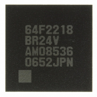
DF2218BR24V Renesas Electronics America, DF2218BR24V Datasheet - Page 519

DF2218BR24V
Manufacturer Part Number
DF2218BR24V
Description
IC H8S/2218 MCU FLASH 112-LFBGA
Manufacturer
Renesas Electronics America
Series
H8® H8S/2200r
Specifications of DF2218BR24V
Core Processor
H8S/2000
Core Size
16-Bit
Speed
24MHz
Connectivity
SCI, SmartCard, USB
Peripherals
DMA, POR, PWM, WDT
Number Of I /o
69
Program Memory Size
128KB (128K x 8)
Program Memory Type
FLASH
Ram Size
12K x 8
Voltage - Supply (vcc/vdd)
2.7 V ~ 3.6 V
Data Converters
A/D 6x10b
Oscillator Type
External
Operating Temperature
-20°C ~ 75°C
Package / Case
112-LFBGA
For Use With
HS0005KCU11H - EMULATOR E10A-USB H8S(X),SH2(A)3DK2218-SS - KIT DEV H8S/2218 WINDOWS SIDESHW3DK2218 - DEV EVAL KIT H8S/2218
Lead Free Status / RoHS Status
Lead free / RoHS Compliant
Eeprom Size
-
Available stocks
Company
Part Number
Manufacturer
Quantity
Price
Company:
Part Number:
DF2218BR24V
Manufacturer:
Renesas Electronics America
Quantity:
10 000
- Current page: 519 of 758
- Download datasheet (5Mb)
13.5
1. When using the boundary scan function, clear TRST to 0 at power-on and after the t
2. The following must be noted on the power-on reset signal applied to the TRST pin.
3. TCK clock speed should be slower than system clock frequency.
4. In serial communication, data is input or output from the LSB as shown in figure 13.5.
has elapsed set TRST to 1 and set TCK, TMS, and TDI appropriately. During normal operation
when the boundary scan function is not used, set TCK, TMS, and TDI to Hi-Z, clear TRST to 0
at power-on, and after the t
pulled up internally, so care must be taken in standby mode because breakthrough current flow
can occur if there is a potential difference between the pin input voltage value when set to 1
and the power supply voltage Vcc.
• Reset signal must be applied at power-on.
• TRST must be separated in order not to affect the system operation.
• TRST must be separated from the system circuitry in order not to affect the system
• System circuitry must also be separated from the TRST in order not to affect TRST
operation.
operation as shown in figure 13.4.
Usage Notes
System
reset
TRST
Board edge pin
Figure 13.4 Recommended Reset Signal Design
Figure 13.5 Serial Data Input/Output
RESW
Boundary scan register
Power-on
reset circuit
time has elapsed set TRST to 1 or to Hi-Z. These pins are
TDI
TDO
Rev.7.00 Dec. 24, 2008 Page 463 of 698
Bit n
Bit n - 1
Bit 1
Bit 0
RES
TRST
LSI
REJ09B0074-0700
RESW
time
Related parts for DF2218BR24V
Image
Part Number
Description
Manufacturer
Datasheet
Request
R

Part Number:
Description:
CONN SOCKET 2POS 7.92MM WHITE
Manufacturer:
Hirose Electric Co Ltd
Datasheet:

Part Number:
Description:
CONN SOCKET 4POS 7.92MM WHITE
Manufacturer:
Hirose Electric Co Ltd
Datasheet:

Part Number:
Description:
CONN SOCKET 5POS 7.92MM WHITE
Manufacturer:
Hirose Electric Co Ltd
Datasheet:

Part Number:
Description:
CONN SOCKET 3POS 7.92MM WHITE
Manufacturer:
Hirose Electric Co Ltd
Datasheet:

Part Number:
Description:
CONN SOCKET 5POS 7.92MM WHITE
Manufacturer:
Hirose Electric Co Ltd
Datasheet:

Part Number:
Description:
CONN SOCKET 2POS 7.92MM WHITE
Manufacturer:
Hirose Electric Co Ltd
Datasheet:

Part Number:
Description:
CONN SOCKET 3POS 7.92MM WHITE
Manufacturer:
Hirose Electric Co Ltd
Datasheet:

Part Number:
Description:
CONN SOCKET 4POS 7.92MM WHITE
Manufacturer:
Hirose Electric Co Ltd
Datasheet:

Part Number:
Description:
CONN HEADER 2POS 7.92MM R/A TIN
Manufacturer:
Hirose Electric Co Ltd
Datasheet:

Part Number:
Description:
CONN HEADER 4POS 7.92MM R/A TIN
Manufacturer:
Hirose Electric Co Ltd
Datasheet:

Part Number:
Description:
KIT STARTER FOR M16C/29
Manufacturer:
Renesas Electronics America
Datasheet:

Part Number:
Description:
KIT STARTER FOR R8C/2D
Manufacturer:
Renesas Electronics America
Datasheet:

Part Number:
Description:
R0K33062P STARTER KIT
Manufacturer:
Renesas Electronics America
Datasheet:

Part Number:
Description:
KIT STARTER FOR R8C/23 E8A
Manufacturer:
Renesas Electronics America
Datasheet:

Part Number:
Description:
KIT STARTER FOR R8C/25
Manufacturer:
Renesas Electronics America
Datasheet:


