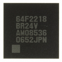
DF2218BR24V Renesas Electronics America, DF2218BR24V Datasheet - Page 639

DF2218BR24V
Manufacturer Part Number
DF2218BR24V
Description
IC H8S/2218 MCU FLASH 112-LFBGA
Manufacturer
Renesas Electronics America
Series
H8® H8S/2200r
Specifications of DF2218BR24V
Core Processor
H8S/2000
Core Size
16-Bit
Speed
24MHz
Connectivity
SCI, SmartCard, USB
Peripherals
DMA, POR, PWM, WDT
Number Of I /o
69
Program Memory Size
128KB (128K x 8)
Program Memory Type
FLASH
Ram Size
12K x 8
Voltage - Supply (vcc/vdd)
2.7 V ~ 3.6 V
Data Converters
A/D 6x10b
Oscillator Type
External
Operating Temperature
-20°C ~ 75°C
Package / Case
112-LFBGA
For Use With
HS0005KCU11H - EMULATOR E10A-USB H8S(X),SH2(A)3DK2218-SS - KIT DEV H8S/2218 WINDOWS SIDESHW3DK2218 - DEV EVAL KIT H8S/2218
Lead Free Status / RoHS Status
Lead free / RoHS Compliant
Eeprom Size
-
Available stocks
Company
Part Number
Manufacturer
Quantity
Price
Company:
Part Number:
DF2218BR24V
Manufacturer:
Renesas Electronics America
Quantity:
10 000
- Current page: 639 of 758
- Download datasheet (5Mb)
17.9
There are three kinds of flash memory program/erase protection: hardware protection, software
protection, and error protection.
17.9.1
Hardware protection refers to a state in which programming/erasing of flash memory is forcibly
disabled or aborted because of a transition to reset or standby mode. Flash memory control
register 1 (FLMCR1), flash memory control register 2 (FLMCR2), erase block register 1 (EBR1),
and erase block register 2 (EBR2) are initialized. In a reset via the RES pin, the reset state is not
entered unless the RES pin is held low until oscillation stabilizes after powering on. In the case of
a reset during operation, hold the RES pin low for the RES pulse width specified in the AC
Characteristics section.
17.9.2
Software protection can be implemented against programming/erasing of all flash memory blocks
by clearing the SWE1 bit in FLMCR1. When software protection is in effect, setting the P1 or E1
bit in FLMCR1 does not cause a transition to program mode or erase mode. By setting the erase
block register 1 (EBR1), and erase block register 2 (EBR2), erase protection can be set for
individual blocks. When EBR1 and EBR2 are set to H'00, erase protection is set for all blocks.
17.9.3
In error protection, an error is detected when the CPU's runaway occurs during flash memory
programming/erasing, or operation is not performed in accordance with the program/erase
algorithm, and the program/erase operation is aborted. Aborting the program/erase operation
prevents damage to the flash memory due to overprogramming or overerasing.
When the following errors are detected during programming/erasing of flash memory, the FLER
bit in FLMCR2 is set to 1, and the error protection state is entered.
Setting Conditions of FLER Bit (Erase Protection)
• When the flash memory of the relevant address area is read during programming/erasing
• Immediately after exception handling (excluding a reset) during programming/erasing
• When a SLEEP instruction is executed during programming/erasing
• When the CPU releases the bus mastership to the DMAC during programming/erasing
(including vector read and instruction fetch)
Program/Erase Protection
Hardware Protection
Software Protection
Error Protection
Rev.7.00 Dec. 24, 2008 Page 583 of 698
REJ09B0074-0700
Related parts for DF2218BR24V
Image
Part Number
Description
Manufacturer
Datasheet
Request
R

Part Number:
Description:
CONN SOCKET 2POS 7.92MM WHITE
Manufacturer:
Hirose Electric Co Ltd
Datasheet:

Part Number:
Description:
CONN SOCKET 4POS 7.92MM WHITE
Manufacturer:
Hirose Electric Co Ltd
Datasheet:

Part Number:
Description:
CONN SOCKET 5POS 7.92MM WHITE
Manufacturer:
Hirose Electric Co Ltd
Datasheet:

Part Number:
Description:
CONN SOCKET 3POS 7.92MM WHITE
Manufacturer:
Hirose Electric Co Ltd
Datasheet:

Part Number:
Description:
CONN SOCKET 5POS 7.92MM WHITE
Manufacturer:
Hirose Electric Co Ltd
Datasheet:

Part Number:
Description:
CONN SOCKET 2POS 7.92MM WHITE
Manufacturer:
Hirose Electric Co Ltd
Datasheet:

Part Number:
Description:
CONN SOCKET 3POS 7.92MM WHITE
Manufacturer:
Hirose Electric Co Ltd
Datasheet:

Part Number:
Description:
CONN SOCKET 4POS 7.92MM WHITE
Manufacturer:
Hirose Electric Co Ltd
Datasheet:

Part Number:
Description:
CONN HEADER 2POS 7.92MM R/A TIN
Manufacturer:
Hirose Electric Co Ltd
Datasheet:

Part Number:
Description:
CONN HEADER 4POS 7.92MM R/A TIN
Manufacturer:
Hirose Electric Co Ltd
Datasheet:

Part Number:
Description:
KIT STARTER FOR M16C/29
Manufacturer:
Renesas Electronics America
Datasheet:

Part Number:
Description:
KIT STARTER FOR R8C/2D
Manufacturer:
Renesas Electronics America
Datasheet:

Part Number:
Description:
R0K33062P STARTER KIT
Manufacturer:
Renesas Electronics America
Datasheet:

Part Number:
Description:
KIT STARTER FOR R8C/23 E8A
Manufacturer:
Renesas Electronics America
Datasheet:

Part Number:
Description:
KIT STARTER FOR R8C/25
Manufacturer:
Renesas Electronics America
Datasheet:


