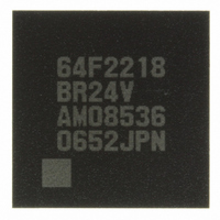
DF2218BR24V Renesas Electronics America, DF2218BR24V Datasheet - Page 628

DF2218BR24V
Manufacturer Part Number
DF2218BR24V
Description
IC H8S/2218 MCU FLASH 112-LFBGA
Manufacturer
Renesas Electronics America
Series
H8® H8S/2200r
Specifications of DF2218BR24V
Core Processor
H8S/2000
Core Size
16-Bit
Speed
24MHz
Connectivity
SCI, SmartCard, USB
Peripherals
DMA, POR, PWM, WDT
Number Of I /o
69
Program Memory Size
128KB (128K x 8)
Program Memory Type
FLASH
Ram Size
12K x 8
Voltage - Supply (vcc/vdd)
2.7 V ~ 3.6 V
Data Converters
A/D 6x10b
Oscillator Type
External
Operating Temperature
-20°C ~ 75°C
Package / Case
112-LFBGA
For Use With
HS0005KCU11H - EMULATOR E10A-USB H8S(X),SH2(A)3DK2218-SS - KIT DEV H8S/2218 WINDOWS SIDESHW3DK2218 - DEV EVAL KIT H8S/2218
Lead Free Status / RoHS Status
Lead free / RoHS Compliant
Eeprom Size
-
Available stocks
Company
Part Number
Manufacturer
Quantity
Price
Company:
Part Number:
DF2218BR24V
Manufacturer:
Renesas Electronics America
Quantity:
10 000
- Current page: 628 of 758
- Download datasheet (5Mb)
• Overview
1. When boot mode is used, the flash memory programming control program must be prepared in
2. When the boot program is activated, enumeration with respect to the host is carried out.
Rev.7.00 Dec. 24, 2008 Page 572 of 698
REJ09B0074-0700
Legend:
×: Don’t care
Note: * FWE pin and mode pin input must satisfy the mode programming setup time (t
self-powerd HUB
When a reset start preformed after the pins of this LSI have been set to boot mode, a boot
program incorporated in the microcomputer beforehand is activated, and the prepared
programming control program is transmitted sequentially to the host using the USB. With this
LSI, the programming control program received by the USB is written to a programming
control program area in on-chip RAM. After transfer is completed, control branches to the start
address of the programming control program area, and the programming control program
execution state is established (flash memory programming is performed). Figure 17.9 shows a
system configuration diagram when using USB boot mode.
Table 17.7 shows operations from reset release in USB boot mode until processing branches to
the programming control program.
the host beforehand. Prepare a programming control program in accordance with the
description in section 17.8, Flash Memory Programming/Erasing. In boot mode, if any data has
been programmed into the flash memory (if all data is not 1), all flash memory blocks are
erased. Boot mode is for use in enforced exit when user program mode is unavailable, such a
the first time on-board programming control program, or performed, or if the program
activated in user program mode is accidentally erased.
Enumeration information is shown in table 17.6. When enumeration is completed, transmit a
single H'55 byte from the host. If reception has not been preformed normally, restart boot mode
by means of a reset.
Host or
Figure 17.9 System Configuration Diagram when Using USB Boot Mode
D+
D-
Data transmission/reception
1.5kΩ
01×
Rs
Rs
0
1
USD+
USD-
EMLE
FWE*
MD2 to MD0*
P36
VBUS
USB
Flash memory
This LSI
On-chip RAM
MDS
EXTAL
UBPM
= 200ns) when a reset is released.
XTAL
1: Self power setting
0: Bus power setting
System clock:
16 MHz or 24MHz
Related parts for DF2218BR24V
Image
Part Number
Description
Manufacturer
Datasheet
Request
R

Part Number:
Description:
CONN SOCKET 2POS 7.92MM WHITE
Manufacturer:
Hirose Electric Co Ltd
Datasheet:

Part Number:
Description:
CONN SOCKET 4POS 7.92MM WHITE
Manufacturer:
Hirose Electric Co Ltd
Datasheet:

Part Number:
Description:
CONN SOCKET 5POS 7.92MM WHITE
Manufacturer:
Hirose Electric Co Ltd
Datasheet:

Part Number:
Description:
CONN SOCKET 3POS 7.92MM WHITE
Manufacturer:
Hirose Electric Co Ltd
Datasheet:

Part Number:
Description:
CONN SOCKET 5POS 7.92MM WHITE
Manufacturer:
Hirose Electric Co Ltd
Datasheet:

Part Number:
Description:
CONN SOCKET 2POS 7.92MM WHITE
Manufacturer:
Hirose Electric Co Ltd
Datasheet:

Part Number:
Description:
CONN SOCKET 3POS 7.92MM WHITE
Manufacturer:
Hirose Electric Co Ltd
Datasheet:

Part Number:
Description:
CONN SOCKET 4POS 7.92MM WHITE
Manufacturer:
Hirose Electric Co Ltd
Datasheet:

Part Number:
Description:
CONN HEADER 2POS 7.92MM R/A TIN
Manufacturer:
Hirose Electric Co Ltd
Datasheet:

Part Number:
Description:
CONN HEADER 4POS 7.92MM R/A TIN
Manufacturer:
Hirose Electric Co Ltd
Datasheet:

Part Number:
Description:
KIT STARTER FOR M16C/29
Manufacturer:
Renesas Electronics America
Datasheet:

Part Number:
Description:
KIT STARTER FOR R8C/2D
Manufacturer:
Renesas Electronics America
Datasheet:

Part Number:
Description:
R0K33062P STARTER KIT
Manufacturer:
Renesas Electronics America
Datasheet:

Part Number:
Description:
KIT STARTER FOR R8C/23 E8A
Manufacturer:
Renesas Electronics America
Datasheet:

Part Number:
Description:
KIT STARTER FOR R8C/25
Manufacturer:
Renesas Electronics America
Datasheet:


