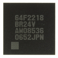
DF2218BR24V Renesas Electronics America, DF2218BR24V Datasheet - Page 324

DF2218BR24V
Manufacturer Part Number
DF2218BR24V
Description
IC H8S/2218 MCU FLASH 112-LFBGA
Manufacturer
Renesas Electronics America
Series
H8® H8S/2200r
Specifications of DF2218BR24V
Core Processor
H8S/2000
Core Size
16-Bit
Speed
24MHz
Connectivity
SCI, SmartCard, USB
Peripherals
DMA, POR, PWM, WDT
Number Of I /o
69
Program Memory Size
128KB (128K x 8)
Program Memory Type
FLASH
Ram Size
12K x 8
Voltage - Supply (vcc/vdd)
2.7 V ~ 3.6 V
Data Converters
A/D 6x10b
Oscillator Type
External
Operating Temperature
-20°C ~ 75°C
Package / Case
112-LFBGA
For Use With
HS0005KCU11H - EMULATOR E10A-USB H8S(X),SH2(A)3DK2218-SS - KIT DEV H8S/2218 WINDOWS SIDESHW3DK2218 - DEV EVAL KIT H8S/2218
Lead Free Status / RoHS Status
Lead free / RoHS Compliant
Eeprom Size
-
Available stocks
Company
Part Number
Manufacturer
Quantity
Price
Company:
Part Number:
DF2218BR24V
Manufacturer:
Renesas Electronics America
Quantity:
10 000
- Current page: 324 of 758
- Download datasheet (5Mb)
8.12.1
PGDDR specifies input or output for the pins of the port G.
Since PGDDR is a write-only register, the bit manipulation instructions must not be used to write
PGDDR. For details, see section 2.9.4, Accessing Registers Containing Write-Only Bits.
Notes: 1. The initial value becomes 1 in modes 4 and 5 and 0 in modes 6 and 7.
Rev.7.00 Dec. 24, 2008 Page 268 of 698
REJ09B0074-0700
Bit
7 to
5
4
3
2
1
0
Bit Name
⎯
PG4DDR*
PG3DDR*
PG2DDR*
PG1DDR
PG0DDR*
2. Reserved in the H8S/2212 Group. If this bit is read, an undefined value will be read.
3. Reserved in the H8S/2218 Group. If this bit is read, an undefined value will be read.
Port G Data Direction Register (PGDDR)
This bit cannot be modified.
This bit cannot be modified.
2
2
2
3
Initial Value
Undefined
0/1*
0
0
0
0
1
R/W
⎯
W
W
W
W
W
Description
Reserved
These bits are undefined and cannot be modified.
(H8S/2218 Group)
Modes 4 to 6:
Setting a PGDDR bit to 1 makes the PG4 to PG1 pins bus
control signal output pins, while clearing the bit to 0
makes the pins input ports.
Mode 7:
Setting a PGDDR bit to 1 makes the corresponding port G
pin an output port, while clearing the bit to 0 makes the
pin an input port.
(H8S/2212 Group)
Setting a PG1DDR bit to 1 makes the corresponding port
G pin an output port, while clearing the bit to 0 makes the
pin an input port.
(H8S/2212 Group)
When EMLE = 1: Pin PG0 function as the H-UDI (TDI)
pin.
When EMLE = 0: If a PG0DDR bit is set to 1, pin PG0
function as output ports. If a PG0DDR bit is cleared to 0,
pin PG0 function as input ports.
Related parts for DF2218BR24V
Image
Part Number
Description
Manufacturer
Datasheet
Request
R

Part Number:
Description:
CONN SOCKET 2POS 7.92MM WHITE
Manufacturer:
Hirose Electric Co Ltd
Datasheet:

Part Number:
Description:
CONN SOCKET 4POS 7.92MM WHITE
Manufacturer:
Hirose Electric Co Ltd
Datasheet:

Part Number:
Description:
CONN SOCKET 5POS 7.92MM WHITE
Manufacturer:
Hirose Electric Co Ltd
Datasheet:

Part Number:
Description:
CONN SOCKET 3POS 7.92MM WHITE
Manufacturer:
Hirose Electric Co Ltd
Datasheet:

Part Number:
Description:
CONN SOCKET 5POS 7.92MM WHITE
Manufacturer:
Hirose Electric Co Ltd
Datasheet:

Part Number:
Description:
CONN SOCKET 2POS 7.92MM WHITE
Manufacturer:
Hirose Electric Co Ltd
Datasheet:

Part Number:
Description:
CONN SOCKET 3POS 7.92MM WHITE
Manufacturer:
Hirose Electric Co Ltd
Datasheet:

Part Number:
Description:
CONN SOCKET 4POS 7.92MM WHITE
Manufacturer:
Hirose Electric Co Ltd
Datasheet:

Part Number:
Description:
CONN HEADER 2POS 7.92MM R/A TIN
Manufacturer:
Hirose Electric Co Ltd
Datasheet:

Part Number:
Description:
CONN HEADER 4POS 7.92MM R/A TIN
Manufacturer:
Hirose Electric Co Ltd
Datasheet:

Part Number:
Description:
KIT STARTER FOR M16C/29
Manufacturer:
Renesas Electronics America
Datasheet:

Part Number:
Description:
KIT STARTER FOR R8C/2D
Manufacturer:
Renesas Electronics America
Datasheet:

Part Number:
Description:
R0K33062P STARTER KIT
Manufacturer:
Renesas Electronics America
Datasheet:

Part Number:
Description:
KIT STARTER FOR R8C/23 E8A
Manufacturer:
Renesas Electronics America
Datasheet:

Part Number:
Description:
KIT STARTER FOR R8C/25
Manufacturer:
Renesas Electronics America
Datasheet:


