DF2265TE13V Renesas Electronics America, DF2265TE13V Datasheet - Page 614
DF2265TE13V
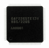
Manufacturer Part Number
DF2265TE13V
Description
IC H8S/2265 MCU FLASH 100TQFP
Manufacturer
Renesas Electronics America
Series
H8® H8S/2200r
Specifications of DF2265TE13V
Core Processor
H8S/2000
Core Size
16-Bit
Speed
13MHz
Connectivity
I²C, SCI, SmartCard
Peripherals
LCD, POR, PWM, WDT
Number Of I /o
67
Program Memory Size
128KB (128K x 8)
Program Memory Type
FLASH
Ram Size
4K x 8
Voltage - Supply (vcc/vdd)
3 V ~ 5.5 V
Data Converters
A/D 10x10b, D/A 2x8b
Oscillator Type
Internal
Operating Temperature
-20°C ~ 75°C
Package / Case
100-TQFP, 100-VQFP
Lead Free Status / RoHS Status
Lead free / RoHS Compliant
Eeprom Size
-
Available stocks
Company
Part Number
Manufacturer
Quantity
Price
Company:

Part Number:
DF2265TE13V
Manufacturer:
Renesas Electronics America
Quantity:
10 000


Section 22 Power-Down Modes
22.4
22.4.1
A transition is made to software standby mode when the SLEEP instruction is executed while the
SBYCR SSBY bit = 1 and the LPWRCR LSON bit = 0, and the TCSR_1 (WDT_1) PSS bit = 0.
In this mode, the CPU, on-chip peripheral modules, and oscillator all stop. However, the contents
of the CPU’s internal registers, RAM data, and the states of on-chip peripheral modules other than
the A/D converter, and the states of I/O ports are retained. In this mode the oscillator stops, and
therefore power dissipation is significantly reduced.
22.4.2
Software standby mode is cleared by an external interrupt (NMI pin, or pins IRQ0, IRQ1, IRQ3,
IRQ4 , IRQ5 * , WKP0 to WKP7), or by means of the RES pin or STBY pin.
• Clearing with an interrupt
• Clearing with the RES pin
• Clearing with the STBY pin
Note: * Supported only by the H8S/2268 Group.
Rev. 5.00 Sep. 01, 2009 Page 562 of 656
REJ09B0071-0500
When an NMI, or IRQ0, IRQ1, IRQ3, IRQ4, IRQ5 * , or WKP0 to WKP7 interrupt request
signal is input, clock oscillation starts, and after the elapse of the time set in bits STS2 to STS0
in SYSCR, stable clocks are supplied to the entire chip, software standby mode is cleared, and
interrupt exception handling is started.
When clearing software standby mode with an IRQ0, IRQ1, IRQ3, IRQ4, IRQ5 * , or WKP0 to
WKP7 interrupt, set the corresponding enable bit/pin function switching bit to 1 and ensure
that no interrupt with a higher priority than interrupts IRQ0, IRQ1, IRQ3, IRQ4, IRQ5 * , or
WKP0 to WKP7 is generated. Software standby mode cannot be cleared if the interrupt has
been masked on the CPU side or has been designated as a DTC activation source.
When the RES pin is driven low, clock oscillation is started. At the same time as clock
oscillation starts, clocks are supplied to the entire chip. Note that the RES pin must be held low
until clock oscillation settles. When the RES pin goes high, the CPU begins reset exception
handling.
When the STBY pin is driven low, a transition is made to hardware standby mode.
Software Standby Mode
Software Standby Mode
Clearing Software Standby Mode
Related parts for DF2265TE13V
Image
Part Number
Description
Manufacturer
Datasheet
Request
R

Part Number:
Description:
CONN SOCKET 2POS 7.92MM WHITE
Manufacturer:
Hirose Electric Co Ltd
Datasheet:

Part Number:
Description:
CONN SOCKET 4POS 7.92MM WHITE
Manufacturer:
Hirose Electric Co Ltd
Datasheet:

Part Number:
Description:
CONN SOCKET 5POS 7.92MM WHITE
Manufacturer:
Hirose Electric Co Ltd
Datasheet:

Part Number:
Description:
CONN SOCKET 3POS 7.92MM WHITE
Manufacturer:
Hirose Electric Co Ltd
Datasheet:
Part Number:
Description:
CONN SOCKET 5POS 7.92MM WHITE
Manufacturer:
Hirose Electric Co Ltd
Datasheet:

Part Number:
Description:
CONN SOCKET 2POS 7.92MM WHITE
Manufacturer:
Hirose Electric Co Ltd
Datasheet:
Part Number:
Description:
CONN SOCKET 3POS 7.92MM WHITE
Manufacturer:
Hirose Electric Co Ltd
Datasheet:
Part Number:
Description:
CONN SOCKET 4POS 7.92MM WHITE
Manufacturer:
Hirose Electric Co Ltd
Datasheet:

Part Number:
Description:
CONN HEADER 2POS 7.92MM R/A TIN
Manufacturer:
Hirose Electric Co Ltd
Datasheet:

Part Number:
Description:
CONN HEADER 4POS 7.92MM R/A TIN
Manufacturer:
Hirose Electric Co Ltd
Datasheet:

Part Number:
Description:
KIT STARTER FOR M16C/29
Manufacturer:
Renesas Electronics America
Datasheet:

Part Number:
Description:
KIT STARTER FOR R8C/2D
Manufacturer:
Renesas Electronics America
Datasheet:

Part Number:
Description:
R0K33062P STARTER KIT
Manufacturer:
Renesas Electronics America
Datasheet:

Part Number:
Description:
KIT STARTER FOR R8C/23 E8A
Manufacturer:
Renesas Electronics America
Datasheet:

Part Number:
Description:
KIT STARTER FOR R8C/25
Manufacturer:
Renesas Electronics America
Datasheet: