DF2265TE13V Renesas Electronics America, DF2265TE13V Datasheet - Page 48
DF2265TE13V
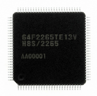
Manufacturer Part Number
DF2265TE13V
Description
IC H8S/2265 MCU FLASH 100TQFP
Manufacturer
Renesas Electronics America
Series
H8® H8S/2200r
Specifications of DF2265TE13V
Core Processor
H8S/2000
Core Size
16-Bit
Speed
13MHz
Connectivity
I²C, SCI, SmartCard
Peripherals
LCD, POR, PWM, WDT
Number Of I /o
67
Program Memory Size
128KB (128K x 8)
Program Memory Type
FLASH
Ram Size
4K x 8
Voltage - Supply (vcc/vdd)
3 V ~ 5.5 V
Data Converters
A/D 10x10b, D/A 2x8b
Oscillator Type
Internal
Operating Temperature
-20°C ~ 75°C
Package / Case
100-TQFP, 100-VQFP
Lead Free Status / RoHS Status
Lead free / RoHS Compliant
Eeprom Size
-
Available stocks
Company
Part Number
Manufacturer
Quantity
Price
Company:

Part Number:
DF2265TE13V
Manufacturer:
Renesas Electronics America
Quantity:
10 000


Section 1 Overview
Table 1.1
Section 2 CPU
Table 2.1
Table 2.2
Table 2.3
Table 2.4
Table 2.4
Table 2.5
Table 2.6
Table 2.7
Table 2.7
Table 2.8
Table 2.9
Table 2.10
Table 2.11
Table 2.12
Table 2.13
Table 2.13
Section 3 MCU Operating Modes
Table 3.1
Section 4 Exception Handling
Table 4.1
Table 4.2
Table 4.3
Table 4.4
Section 5 Interrupt Controller
Table 5.1
Table 5.2
Table 5.3
Table 5.4
Table 5.5
Table 5.6
Table 5.7
Rev. 5.00 Sep. 01, 2009 Page xlvi of l
REJ09B0071-0500
Pin Functions..............................................................................................................7
Instruction Classification..........................................................................................29
Operation Notation...................................................................................................30
Data Transfer Instructions ........................................................................................31
Arithmetic Operations Instructions (1).....................................................................32
Arithmetic Operations Instructions (2).....................................................................33
Logic Operations Instructions ..................................................................................34
Shift Instructions ......................................................................................................34
Bit Manipulation Instructions (1) .............................................................................35
Bit Manipulation Instructions (2) .............................................................................36
Branch Instructions ..................................................................................................37
System Control Instructions .....................................................................................38
Block Data Transfer Instructions..............................................................................39
Addressing Modes....................................................................................................41
Absolute Address Access Ranges ............................................................................42
Effective Address Calculation (1) ............................................................................45
Effective Address Calculation (2) ............................................................................46
MCU Operating Mode Selection..............................................................................55
Exception Types and Priority ...................................................................................59
Exception Handling Vector Table ............................................................................60
Status of CCR and EXR after Trace Exception Handling ........................................63
Status of CCR and EXR after Trap Instruction Exception Handling .......................64
Pin Configuration .....................................................................................................70
Interrupt Sources, Vector Addresses, and Interrupt Priorities ..................................85
Interrupt Control Modes...........................................................................................89
Interrupts Selected in Each Interrupt Control Mode (1)...........................................90
Interrupts Selected in Each Interrupt Control Mode (2)...........................................90
Operations and Control Signal Functions in Each Interrupt Control Mode .............91
Interrupt Response Times (States)............................................................................97
Tables
Related parts for DF2265TE13V
Image
Part Number
Description
Manufacturer
Datasheet
Request
R

Part Number:
Description:
CONN SOCKET 2POS 7.92MM WHITE
Manufacturer:
Hirose Electric Co Ltd
Datasheet:

Part Number:
Description:
CONN SOCKET 4POS 7.92MM WHITE
Manufacturer:
Hirose Electric Co Ltd
Datasheet:

Part Number:
Description:
CONN SOCKET 5POS 7.92MM WHITE
Manufacturer:
Hirose Electric Co Ltd
Datasheet:

Part Number:
Description:
CONN SOCKET 3POS 7.92MM WHITE
Manufacturer:
Hirose Electric Co Ltd
Datasheet:
Part Number:
Description:
CONN SOCKET 5POS 7.92MM WHITE
Manufacturer:
Hirose Electric Co Ltd
Datasheet:

Part Number:
Description:
CONN SOCKET 2POS 7.92MM WHITE
Manufacturer:
Hirose Electric Co Ltd
Datasheet:
Part Number:
Description:
CONN SOCKET 3POS 7.92MM WHITE
Manufacturer:
Hirose Electric Co Ltd
Datasheet:
Part Number:
Description:
CONN SOCKET 4POS 7.92MM WHITE
Manufacturer:
Hirose Electric Co Ltd
Datasheet:

Part Number:
Description:
CONN HEADER 2POS 7.92MM R/A TIN
Manufacturer:
Hirose Electric Co Ltd
Datasheet:

Part Number:
Description:
CONN HEADER 4POS 7.92MM R/A TIN
Manufacturer:
Hirose Electric Co Ltd
Datasheet:

Part Number:
Description:
KIT STARTER FOR M16C/29
Manufacturer:
Renesas Electronics America
Datasheet:

Part Number:
Description:
KIT STARTER FOR R8C/2D
Manufacturer:
Renesas Electronics America
Datasheet:

Part Number:
Description:
R0K33062P STARTER KIT
Manufacturer:
Renesas Electronics America
Datasheet:

Part Number:
Description:
KIT STARTER FOR R8C/23 E8A
Manufacturer:
Renesas Electronics America
Datasheet:

Part Number:
Description:
KIT STARTER FOR R8C/25
Manufacturer:
Renesas Electronics America
Datasheet: