DF2265TE13V Renesas Electronics America, DF2265TE13V Datasheet - Page 462
DF2265TE13V
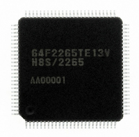
Manufacturer Part Number
DF2265TE13V
Description
IC H8S/2265 MCU FLASH 100TQFP
Manufacturer
Renesas Electronics America
Series
H8® H8S/2200r
Specifications of DF2265TE13V
Core Processor
H8S/2000
Core Size
16-Bit
Speed
13MHz
Connectivity
I²C, SCI, SmartCard
Peripherals
LCD, POR, PWM, WDT
Number Of I /o
67
Program Memory Size
128KB (128K x 8)
Program Memory Type
FLASH
Ram Size
4K x 8
Voltage - Supply (vcc/vdd)
3 V ~ 5.5 V
Data Converters
A/D 10x10b, D/A 2x8b
Oscillator Type
Internal
Operating Temperature
-20°C ~ 75°C
Package / Case
100-TQFP, 100-VQFP
Lead Free Status / RoHS Status
Lead free / RoHS Compliant
Eeprom Size
-
Available stocks
Company
Part Number
Manufacturer
Quantity
Price
Company:

Part Number:
DF2265TE13V
Manufacturer:
Renesas Electronics America
Quantity:
10 000


Section 14 I
The transmission procedure and operations synchronized with the ICDR writing are described
below.
1. Perform initial settings as described in section 14.4.2, Initial Setting.
2. Read the BBSY flag in ICCR to confirm that the bus is free.
3. Set bits MST and TRS to 1 in ICCR to select master transmit mode.
4. Write 1 to BBSY and 0 to SCP. This changes SDA from high to low when SCL is high, and
5. Then IRIC and IRTR flags are set to 1. If the IEIC bit in ICCR has been set to 1, an interrupt
6. After the start condition is detected, write the data (slave address + R/W) to ICDR. With the
7. When one frame of data has been transmitted, the IRIC flag is set to 1 at the rise of the 9th
8. Read the ACKB bit in ICSR to confirm that ACKB is cleared to 0. When the slave device has
9. Write the transmit data to ICDR. As indicating the end of the transfer, and so the IRIC flag is
10. When one frame of data has been transmitted, the IRIC flag is set to 1 at the rise of the 9th
11. Read the ACKB bit in ICSR. Confirm that the slave device has been acknowledged (ACKB bit
Rev. 5.00 Sep. 01, 2009 Page 410 of 656
REJ09B0071-0500
generates the start condition.
request is sent to the CPU.
I
following the start condition indicates the 7-bit slave address and transmit/receive direction
(R/W). As indicating the end of the transfer, and so the IRIC flag is cleared to 0. After writing
ICDR, clear IRIC continuously not to execute other interrupt handling routine. If one frame of
data has been transmitted before the IRIC clearing, it can not be determine the end of
transmission. The master device sequentially sends the transmission clock and the data written
to ICDR using the timing shown in figure 14.8. The selected slave device (i.e. the slave device
with the matching slave address) drives SDA low at the 9th transmit clock pulse and returns an
acknowledge signal.
transmit clock pulse. After one frame has been transmitted SCL is automatically fixed low in
synchronization with the internal clock until the next transmit data is written.
not acknowledged (ACKB bit is 1), operate the step [12] to end transmission, and retry the
transmit operation.
cleared to 0. Perform the ICDR write and the IRIC flag clearing sequentially, just as in point 6
in this flowchart. Transmission of the next frame is performed in synchronization with the
internal clock.
transmit clock pulse. After one frame has been transmitted SCL is automatically fixed low in
synchronization with the internal clock until the next transmit data is written.
is 0). When there is data to be transmitted, go to the step [9] to continue next transmission.
When the slave device has not acknowledged (ACKB bit is set to 1), operate the step [12] to
end transmission.
2
C bus format (when the FS bit in SAR or the FSX bit in SARX is 0), the first frame data
2
C Bus Interface (IIC) (Supported as an Option by H8S/2264 Group)
Related parts for DF2265TE13V
Image
Part Number
Description
Manufacturer
Datasheet
Request
R

Part Number:
Description:
CONN SOCKET 2POS 7.92MM WHITE
Manufacturer:
Hirose Electric Co Ltd
Datasheet:

Part Number:
Description:
CONN SOCKET 4POS 7.92MM WHITE
Manufacturer:
Hirose Electric Co Ltd
Datasheet:

Part Number:
Description:
CONN SOCKET 5POS 7.92MM WHITE
Manufacturer:
Hirose Electric Co Ltd
Datasheet:

Part Number:
Description:
CONN SOCKET 3POS 7.92MM WHITE
Manufacturer:
Hirose Electric Co Ltd
Datasheet:
Part Number:
Description:
CONN SOCKET 5POS 7.92MM WHITE
Manufacturer:
Hirose Electric Co Ltd
Datasheet:

Part Number:
Description:
CONN SOCKET 2POS 7.92MM WHITE
Manufacturer:
Hirose Electric Co Ltd
Datasheet:
Part Number:
Description:
CONN SOCKET 3POS 7.92MM WHITE
Manufacturer:
Hirose Electric Co Ltd
Datasheet:
Part Number:
Description:
CONN SOCKET 4POS 7.92MM WHITE
Manufacturer:
Hirose Electric Co Ltd
Datasheet:

Part Number:
Description:
CONN HEADER 2POS 7.92MM R/A TIN
Manufacturer:
Hirose Electric Co Ltd
Datasheet:

Part Number:
Description:
CONN HEADER 4POS 7.92MM R/A TIN
Manufacturer:
Hirose Electric Co Ltd
Datasheet:

Part Number:
Description:
KIT STARTER FOR M16C/29
Manufacturer:
Renesas Electronics America
Datasheet:

Part Number:
Description:
KIT STARTER FOR R8C/2D
Manufacturer:
Renesas Electronics America
Datasheet:

Part Number:
Description:
R0K33062P STARTER KIT
Manufacturer:
Renesas Electronics America
Datasheet:

Part Number:
Description:
KIT STARTER FOR R8C/23 E8A
Manufacturer:
Renesas Electronics America
Datasheet:

Part Number:
Description:
KIT STARTER FOR R8C/25
Manufacturer:
Renesas Electronics America
Datasheet: