DF2265TE13V Renesas Electronics America, DF2265TE13V Datasheet - Page 425
DF2265TE13V
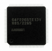
Manufacturer Part Number
DF2265TE13V
Description
IC H8S/2265 MCU FLASH 100TQFP
Manufacturer
Renesas Electronics America
Series
H8® H8S/2200r
Specifications of DF2265TE13V
Core Processor
H8S/2000
Core Size
16-Bit
Speed
13MHz
Connectivity
I²C, SCI, SmartCard
Peripherals
LCD, POR, PWM, WDT
Number Of I /o
67
Program Memory Size
128KB (128K x 8)
Program Memory Type
FLASH
Ram Size
4K x 8
Voltage - Supply (vcc/vdd)
3 V ~ 5.5 V
Data Converters
A/D 10x10b, D/A 2x8b
Oscillator Type
Internal
Operating Temperature
-20°C ~ 75°C
Package / Case
100-TQFP, 100-VQFP
Lead Free Status / RoHS Status
Lead free / RoHS Compliant
Eeprom Size
-
Available stocks
Company
Part Number
Manufacturer
Quantity
Price
Company:

Part Number:
DF2265TE13V
Manufacturer:
Renesas Electronics America
Quantity:
10 000


When turning on the power or switching between Smart Card interface mode and software
standby mode, the following procedures should be followed in order to maintain the clock duty.
Powering on: To secure clock duty from power-on, the following switching procedure should be
followed.
1. The initial state is port input and high impedance. Use a pull-up resistor or pull-down resistor
2. Fix the SCK pin to the specified output level with the CKE1 bit in SCR.
3. Set SMR and SCMR, and switch to smart card mode operation.
4. Set the CKE0 bit in SCR to 1 to start clock output.
When changing from smart card interface mode to software standby mode:
1. Set the data register (DR) and data direction register (DDR) corresponding to the SCK pin to
2. Write 0 to the TE bit and RE bit in the serial control register (SCR) to halt transmit/receive
3. Write 0 to the CKE0 bit in SCR to halt the clock.
4. Wait for one serial clock period.
5. Make the transition to the software standby state.
to fix the potential.
the value for the fixed output state in software standby mode.
operation. At the same time, set the CKE1 bit to the value for the fixed output state in software
standby mode.
During this interval, clock output is fixed at the specified level, with the duty preserved.
CKE0
SCK
Figure 13.34 Timing for Fixing Clock Output Level
Specified pulse width
Section 13 Serial Communication Interface (SCI)
Rev. 5.00 Sep. 01, 2009 Page 373 of 656
Specified pulse width
REJ09B0071-0500
Related parts for DF2265TE13V
Image
Part Number
Description
Manufacturer
Datasheet
Request
R

Part Number:
Description:
CONN SOCKET 2POS 7.92MM WHITE
Manufacturer:
Hirose Electric Co Ltd
Datasheet:

Part Number:
Description:
CONN SOCKET 4POS 7.92MM WHITE
Manufacturer:
Hirose Electric Co Ltd
Datasheet:

Part Number:
Description:
CONN SOCKET 5POS 7.92MM WHITE
Manufacturer:
Hirose Electric Co Ltd
Datasheet:

Part Number:
Description:
CONN SOCKET 3POS 7.92MM WHITE
Manufacturer:
Hirose Electric Co Ltd
Datasheet:
Part Number:
Description:
CONN SOCKET 5POS 7.92MM WHITE
Manufacturer:
Hirose Electric Co Ltd
Datasheet:

Part Number:
Description:
CONN SOCKET 2POS 7.92MM WHITE
Manufacturer:
Hirose Electric Co Ltd
Datasheet:
Part Number:
Description:
CONN SOCKET 3POS 7.92MM WHITE
Manufacturer:
Hirose Electric Co Ltd
Datasheet:
Part Number:
Description:
CONN SOCKET 4POS 7.92MM WHITE
Manufacturer:
Hirose Electric Co Ltd
Datasheet:

Part Number:
Description:
CONN HEADER 2POS 7.92MM R/A TIN
Manufacturer:
Hirose Electric Co Ltd
Datasheet:

Part Number:
Description:
CONN HEADER 4POS 7.92MM R/A TIN
Manufacturer:
Hirose Electric Co Ltd
Datasheet:

Part Number:
Description:
KIT STARTER FOR M16C/29
Manufacturer:
Renesas Electronics America
Datasheet:

Part Number:
Description:
KIT STARTER FOR R8C/2D
Manufacturer:
Renesas Electronics America
Datasheet:

Part Number:
Description:
R0K33062P STARTER KIT
Manufacturer:
Renesas Electronics America
Datasheet:

Part Number:
Description:
KIT STARTER FOR R8C/23 E8A
Manufacturer:
Renesas Electronics America
Datasheet:

Part Number:
Description:
KIT STARTER FOR R8C/25
Manufacturer:
Renesas Electronics America
Datasheet: