DF2265TE13V Renesas Electronics America, DF2265TE13V Datasheet - Page 208
DF2265TE13V
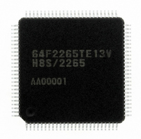
Manufacturer Part Number
DF2265TE13V
Description
IC H8S/2265 MCU FLASH 100TQFP
Manufacturer
Renesas Electronics America
Series
H8® H8S/2200r
Specifications of DF2265TE13V
Core Processor
H8S/2000
Core Size
16-Bit
Speed
13MHz
Connectivity
I²C, SCI, SmartCard
Peripherals
LCD, POR, PWM, WDT
Number Of I /o
67
Program Memory Size
128KB (128K x 8)
Program Memory Type
FLASH
Ram Size
4K x 8
Voltage - Supply (vcc/vdd)
3 V ~ 5.5 V
Data Converters
A/D 10x10b, D/A 2x8b
Oscillator Type
Internal
Operating Temperature
-20°C ~ 75°C
Package / Case
100-TQFP, 100-VQFP
Lead Free Status / RoHS Status
Lead free / RoHS Compliant
Eeprom Size
-
Available stocks
Company
Part Number
Manufacturer
Quantity
Price
Company:

Part Number:
DF2265TE13V
Manufacturer:
Renesas Electronics America
Quantity:
10 000


Section 9 I/O Ports
• P32/SCK0/SDA1 *
Notes: 1. When this pin is used as an external interrupt pin, do not specify other functions.
• P31/RxD0
• P30/TxD0
Rev. 5.00 Sep. 01, 2009 Page 156 of 656
REJ09B0071-0500
ICE *
CKE1
C/A
CKE0
P32DDR
Pin functions
RE
P31DDR
Pin functions
TE
P30DDR
Pin functions
The pin function is switched as shown below according to the combination of the ICE bit *
ICCR_1 of IIC_1, C/A bit in SMR of SCI_0, CKE0 and CKE1 bits in SCR and the P32DDR
bit.
The pin function is switched as shown below according to the combination of the RE bit in
SCR of SCI_0 and the P31DDR bit.
The pin function is switched as shown below according to the combination of the TE bit in
SCR of SCI_0 and the P30DDR bit.
2
2. Supported only by the H8S/2268 Group.
P32 input pin P32 output
2
/IRQ4
0
P31 input pin
P30 input pin
0
0
0
pin
0
1
0
0
0
SCK0 output
pin
0
⎯
P31 output pin
P30 output pin
1
IRQ4 Input *
1
1
SCK0 output
1
pin
⎯
⎯
1
SCK0 input
TxD0 output pin
RxD0 input pin
pin
⎯
⎯
⎯
1
⎯
⎯
1
1
SDA1 I/O
pin *
⎯
1
0
0
0
2
2
in
Related parts for DF2265TE13V
Image
Part Number
Description
Manufacturer
Datasheet
Request
R

Part Number:
Description:
CONN SOCKET 2POS 7.92MM WHITE
Manufacturer:
Hirose Electric Co Ltd
Datasheet:

Part Number:
Description:
CONN SOCKET 4POS 7.92MM WHITE
Manufacturer:
Hirose Electric Co Ltd
Datasheet:

Part Number:
Description:
CONN SOCKET 5POS 7.92MM WHITE
Manufacturer:
Hirose Electric Co Ltd
Datasheet:

Part Number:
Description:
CONN SOCKET 3POS 7.92MM WHITE
Manufacturer:
Hirose Electric Co Ltd
Datasheet:
Part Number:
Description:
CONN SOCKET 5POS 7.92MM WHITE
Manufacturer:
Hirose Electric Co Ltd
Datasheet:

Part Number:
Description:
CONN SOCKET 2POS 7.92MM WHITE
Manufacturer:
Hirose Electric Co Ltd
Datasheet:
Part Number:
Description:
CONN SOCKET 3POS 7.92MM WHITE
Manufacturer:
Hirose Electric Co Ltd
Datasheet:
Part Number:
Description:
CONN SOCKET 4POS 7.92MM WHITE
Manufacturer:
Hirose Electric Co Ltd
Datasheet:

Part Number:
Description:
CONN HEADER 2POS 7.92MM R/A TIN
Manufacturer:
Hirose Electric Co Ltd
Datasheet:

Part Number:
Description:
CONN HEADER 4POS 7.92MM R/A TIN
Manufacturer:
Hirose Electric Co Ltd
Datasheet:

Part Number:
Description:
KIT STARTER FOR M16C/29
Manufacturer:
Renesas Electronics America
Datasheet:

Part Number:
Description:
KIT STARTER FOR R8C/2D
Manufacturer:
Renesas Electronics America
Datasheet:

Part Number:
Description:
R0K33062P STARTER KIT
Manufacturer:
Renesas Electronics America
Datasheet:

Part Number:
Description:
KIT STARTER FOR R8C/23 E8A
Manufacturer:
Renesas Electronics America
Datasheet:

Part Number:
Description:
KIT STARTER FOR R8C/25
Manufacturer:
Renesas Electronics America
Datasheet: