DF2265TE13V Renesas Electronics America, DF2265TE13V Datasheet - Page 408
DF2265TE13V
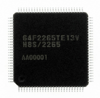
Manufacturer Part Number
DF2265TE13V
Description
IC H8S/2265 MCU FLASH 100TQFP
Manufacturer
Renesas Electronics America
Series
H8® H8S/2200r
Specifications of DF2265TE13V
Core Processor
H8S/2000
Core Size
16-Bit
Speed
13MHz
Connectivity
I²C, SCI, SmartCard
Peripherals
LCD, POR, PWM, WDT
Number Of I /o
67
Program Memory Size
128KB (128K x 8)
Program Memory Type
FLASH
Ram Size
4K x 8
Voltage - Supply (vcc/vdd)
3 V ~ 5.5 V
Data Converters
A/D 10x10b, D/A 2x8b
Oscillator Type
Internal
Operating Temperature
-20°C ~ 75°C
Package / Case
100-TQFP, 100-VQFP
Lead Free Status / RoHS Status
Lead free / RoHS Compliant
Eeprom Size
-
Available stocks
Company
Part Number
Manufacturer
Quantity
Price
Company:

Part Number:
DF2265TE13V
Manufacturer:
Renesas Electronics America
Quantity:
10 000


Section 13 Serial Communication Interface (SCI)
13.6.3
Figure 13.19 shows an example of SCI operation for transmission in clocked synchronous mode.
In serial transmission, the SCI operates as described below.
1. The SCI monitors the TDRE flag in SSR, and if the flag is 0, the SCI recognizes that data has
2. After transferring data from TDR to TSR, the SCI sets the TDRE flag to 1 and starts
Rev. 5.00 Sep. 01, 2009 Page 356 of 656
REJ09B0071-0500
been written to TDR, and transfers the data from TDR to TSR.
transmission. If the TIE bit in SCR is set to 1 at this time, a transmit data empty interrupt
(TXI) is generated. Continuous transmission is possible because the TXI interrupt routine
writes the next transmit data to TDR before transmission of the current transmit data has been
completed.
Note: In simultaneous transmit and receive operations, the TE and RE bits should both be cleared
Serial Data Transmission (Clocked Synchronous Mode)
Set TE and RE bits in SCR to 1, and
set RIE, TIE, TEIE, and MPIE bits
Clear TE and RE bits in SCR to 0
Set CKE1 and CKE0 bits in SCR
to 0 or set to 1 simultaneously.
Set data transfer format in
1-bit interval elapsed?
Start initialization
Set value in BRR
SMR and SCMR
<Transfer start>
(TE, RE bits 0)
Figure 13.18 Sample SCI Initialization Flowchart
Yes
Wait
No
[4]
[2]
[3]
[1]
[1] Set the clock selection in SCR. Be sure
[2] Set the data transfer format in SMR and
[3] Write a value corresponding to the bit
[4] Wait at least one bit interval, then set
to clear bits RIE, TIE, TEIE, and MPIE,
TE and RE, to 0.
SCMR.
rate to BRR. Not necessary if an
external clock is used.
the TE bit or RE bit in SCR to 1.
Also set the RIE, TIE TEIE, and MPIE
bits.
Setting the TE and RE bits enables the
TxD and RxD pins to be used.
Related parts for DF2265TE13V
Image
Part Number
Description
Manufacturer
Datasheet
Request
R

Part Number:
Description:
CONN SOCKET 2POS 7.92MM WHITE
Manufacturer:
Hirose Electric Co Ltd
Datasheet:

Part Number:
Description:
CONN SOCKET 4POS 7.92MM WHITE
Manufacturer:
Hirose Electric Co Ltd
Datasheet:

Part Number:
Description:
CONN SOCKET 5POS 7.92MM WHITE
Manufacturer:
Hirose Electric Co Ltd
Datasheet:

Part Number:
Description:
CONN SOCKET 3POS 7.92MM WHITE
Manufacturer:
Hirose Electric Co Ltd
Datasheet:
Part Number:
Description:
CONN SOCKET 5POS 7.92MM WHITE
Manufacturer:
Hirose Electric Co Ltd
Datasheet:

Part Number:
Description:
CONN SOCKET 2POS 7.92MM WHITE
Manufacturer:
Hirose Electric Co Ltd
Datasheet:
Part Number:
Description:
CONN SOCKET 3POS 7.92MM WHITE
Manufacturer:
Hirose Electric Co Ltd
Datasheet:
Part Number:
Description:
CONN SOCKET 4POS 7.92MM WHITE
Manufacturer:
Hirose Electric Co Ltd
Datasheet:

Part Number:
Description:
CONN HEADER 2POS 7.92MM R/A TIN
Manufacturer:
Hirose Electric Co Ltd
Datasheet:

Part Number:
Description:
CONN HEADER 4POS 7.92MM R/A TIN
Manufacturer:
Hirose Electric Co Ltd
Datasheet:

Part Number:
Description:
KIT STARTER FOR M16C/29
Manufacturer:
Renesas Electronics America
Datasheet:

Part Number:
Description:
KIT STARTER FOR R8C/2D
Manufacturer:
Renesas Electronics America
Datasheet:

Part Number:
Description:
R0K33062P STARTER KIT
Manufacturer:
Renesas Electronics America
Datasheet:

Part Number:
Description:
KIT STARTER FOR R8C/23 E8A
Manufacturer:
Renesas Electronics America
Datasheet:

Part Number:
Description:
KIT STARTER FOR R8C/25
Manufacturer:
Renesas Electronics America
Datasheet: