DF2265TE13V Renesas Electronics America, DF2265TE13V Datasheet - Page 480
DF2265TE13V
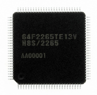
Manufacturer Part Number
DF2265TE13V
Description
IC H8S/2265 MCU FLASH 100TQFP
Manufacturer
Renesas Electronics America
Series
H8® H8S/2200r
Specifications of DF2265TE13V
Core Processor
H8S/2000
Core Size
16-Bit
Speed
13MHz
Connectivity
I²C, SCI, SmartCard
Peripherals
LCD, POR, PWM, WDT
Number Of I /o
67
Program Memory Size
128KB (128K x 8)
Program Memory Type
FLASH
Ram Size
4K x 8
Voltage - Supply (vcc/vdd)
3 V ~ 5.5 V
Data Converters
A/D 10x10b, D/A 2x8b
Oscillator Type
Internal
Operating Temperature
-20°C ~ 75°C
Package / Case
100-TQFP, 100-VQFP
Lead Free Status / RoHS Status
Lead free / RoHS Compliant
Eeprom Size
-
Available stocks
Company
Part Number
Manufacturer
Quantity
Price
Company:

Part Number:
DF2265TE13V
Manufacturer:
Renesas Electronics America
Quantity:
10 000


Section 14 I
The following items are not initialized:
• Actual register values (ICDR, SAR, SARX, ICMR, ICCR, ICSR, DDCSWR, and STCR)
• Internal latches used to retain register read information for setting/clearing flags in the ICMR,
• The value of the ICMR register bit counter (BC2 to BC0)
• Generated interrupt sources (interrupt sources transferred to the interrupt controller)
Notes on Initialization:
• Interrupt flags and interrupt sources are not cleared, and so flag clearing measures must be
• Basically, other register flags are not cleared either, and so flag clearing measures must be
• When initialization is performed by means of the DDCSWR register, the write data for bits
• If a flag clearing setting is made during transmission/reception, the IIC module will stop
The value of the BBSY bit cannot be modified directly by this module clear function, but since the
stop condition pin waveform is generated according to the state and release timing of the SCL and
SDA pins, the BBSY bit may be cleared as a result. Similarly, state switching of other bits and
flags may also have an effect.
To prevent problems caused by these factors, the following procedure should be used when
initializing the IIC state.
1. Execute initialization of the internal state according to the setting of bits CLR3 to CLR0, or
2. Execute a stop condition issuance instruction (write 0 to BBSY and SCP) to clear the BBSY
3. Re-execute initialization of the internal state according to the setting of bits CLR3 to CLR0, or
4. Initialize (re-set) the IIC registers.
Rev. 5.00 Sep. 01, 2009 Page 428 of 656
REJ09B0071-0500
ICCR, ICSR, and DDCSWR registers
taken as necessary.
taken as necessary.
CLR3 to CLR0 is not retained. To perform IIC clearance, bits CLR3 to CLR0 must be written
to simultaneously using an MOV instruction. Do not use a bit manipulation instruction such as
BCLR. Similarly, when clearing is required again, all the bits must be written to
simultaneously in accordance with the setting.
transmitting/receiving at that point and the SCL and SDA pins will be released. When
transmission/reception is started again, register initialization, etc., must be carried out as
necessary to enable correct communication as a system.
according to the ICE bit.
bit to 0, and wait for two transfer rate clock cycles.
according to the ICE bit.
2
C Bus Interface (IIC) (Supported as an Option by H8S/2264 Group)
Related parts for DF2265TE13V
Image
Part Number
Description
Manufacturer
Datasheet
Request
R

Part Number:
Description:
CONN SOCKET 2POS 7.92MM WHITE
Manufacturer:
Hirose Electric Co Ltd
Datasheet:

Part Number:
Description:
CONN SOCKET 4POS 7.92MM WHITE
Manufacturer:
Hirose Electric Co Ltd
Datasheet:

Part Number:
Description:
CONN SOCKET 5POS 7.92MM WHITE
Manufacturer:
Hirose Electric Co Ltd
Datasheet:

Part Number:
Description:
CONN SOCKET 3POS 7.92MM WHITE
Manufacturer:
Hirose Electric Co Ltd
Datasheet:
Part Number:
Description:
CONN SOCKET 5POS 7.92MM WHITE
Manufacturer:
Hirose Electric Co Ltd
Datasheet:

Part Number:
Description:
CONN SOCKET 2POS 7.92MM WHITE
Manufacturer:
Hirose Electric Co Ltd
Datasheet:
Part Number:
Description:
CONN SOCKET 3POS 7.92MM WHITE
Manufacturer:
Hirose Electric Co Ltd
Datasheet:
Part Number:
Description:
CONN SOCKET 4POS 7.92MM WHITE
Manufacturer:
Hirose Electric Co Ltd
Datasheet:

Part Number:
Description:
CONN HEADER 2POS 7.92MM R/A TIN
Manufacturer:
Hirose Electric Co Ltd
Datasheet:

Part Number:
Description:
CONN HEADER 4POS 7.92MM R/A TIN
Manufacturer:
Hirose Electric Co Ltd
Datasheet:

Part Number:
Description:
KIT STARTER FOR M16C/29
Manufacturer:
Renesas Electronics America
Datasheet:

Part Number:
Description:
KIT STARTER FOR R8C/2D
Manufacturer:
Renesas Electronics America
Datasheet:

Part Number:
Description:
R0K33062P STARTER KIT
Manufacturer:
Renesas Electronics America
Datasheet:

Part Number:
Description:
KIT STARTER FOR R8C/23 E8A
Manufacturer:
Renesas Electronics America
Datasheet:

Part Number:
Description:
KIT STARTER FOR R8C/25
Manufacturer:
Renesas Electronics America
Datasheet: