DF2265TE13V Renesas Electronics America, DF2265TE13V Datasheet - Page 543
DF2265TE13V
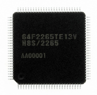
Manufacturer Part Number
DF2265TE13V
Description
IC H8S/2265 MCU FLASH 100TQFP
Manufacturer
Renesas Electronics America
Series
H8® H8S/2200r
Specifications of DF2265TE13V
Core Processor
H8S/2000
Core Size
16-Bit
Speed
13MHz
Connectivity
I²C, SCI, SmartCard
Peripherals
LCD, POR, PWM, WDT
Number Of I /o
67
Program Memory Size
128KB (128K x 8)
Program Memory Type
FLASH
Ram Size
4K x 8
Voltage - Supply (vcc/vdd)
3 V ~ 5.5 V
Data Converters
A/D 10x10b, D/A 2x8b
Oscillator Type
Internal
Operating Temperature
-20°C ~ 75°C
Package / Case
100-TQFP, 100-VQFP
Lead Free Status / RoHS Status
Lead free / RoHS Compliant
Eeprom Size
-
Available stocks
Company
Part Number
Manufacturer
Quantity
Price
Company:

Part Number:
DF2265TE13V
Manufacturer:
Renesas Electronics America
Quantity:
10 000


• Example of Operation (1/3 bias operation)
⎯ During charging period Tc in figure 17.11, the voltages that are divided by the internal
⎯ In the subsequent discharge period Tdc, the charge operation stops. The LCD panel is now
⎯ At this point in time, the respective voltages fall slightly as the capacitors are discharged.
⎯ The capacitors connected to the V1, V2, and V3 terminals are repeatedly charged and
⎯ The capacitance of the capacitors and a charge-discharge period is determined by the
⎯ In actuality, the capacitance of the capacitors and the charge-discharge period must be
division resistors are applied to the V1, V2, and V3 terminals (the V2 voltage is two thirds
of the V1 voltage and the V3 voltage is one third of the V1 voltage), and these voltages
charge external capacitors C1, C2, and C3. Even during this period, the LCD panel is
being driven.
driven by discharge of the charges accumulated in the respective capacitors.
Attention must be paid so that the operation of the LCD panel is not affected, by selecting
the proper charging period and the capacitance of the capacitors.
discharged in the cycles shown in figure 17.11 and retain required voltages, keeping the
LCD panel in operation.
quantity of power in which the LCD panel requires. In addition, the charge-discharge
period can be selected by CDS3 to 0.
determined through experiment, on the basis of the power dissipation specifications of the
LCD panel. This method, however, permits the most proper current value to be selected,
compared with a case in which a DC current continually flows in the internal resistors.
V1
V2
V3
Figure 17.11 Example of Low-Power-Consumption LCD Drive Operation
C3
C2
C1
V1 potential
V2 potential
V3 potential
Power supply voltage fluctuation in 1/3 bias system
period Tc
Charging
V1 × 2/3
V1 × 1/3
Rev. 5.00 Sep. 01, 2009 Page 491 of 656
Discharging
period Tdc
Section 17 LCD Controller/Driver
Vd1
Vd2
Vd3
REJ09B0071-0500
Voltage drop
associated with
discharging due
to LCD panel
driving
Related parts for DF2265TE13V
Image
Part Number
Description
Manufacturer
Datasheet
Request
R

Part Number:
Description:
CONN SOCKET 2POS 7.92MM WHITE
Manufacturer:
Hirose Electric Co Ltd
Datasheet:

Part Number:
Description:
CONN SOCKET 4POS 7.92MM WHITE
Manufacturer:
Hirose Electric Co Ltd
Datasheet:

Part Number:
Description:
CONN SOCKET 5POS 7.92MM WHITE
Manufacturer:
Hirose Electric Co Ltd
Datasheet:

Part Number:
Description:
CONN SOCKET 3POS 7.92MM WHITE
Manufacturer:
Hirose Electric Co Ltd
Datasheet:
Part Number:
Description:
CONN SOCKET 5POS 7.92MM WHITE
Manufacturer:
Hirose Electric Co Ltd
Datasheet:

Part Number:
Description:
CONN SOCKET 2POS 7.92MM WHITE
Manufacturer:
Hirose Electric Co Ltd
Datasheet:
Part Number:
Description:
CONN SOCKET 3POS 7.92MM WHITE
Manufacturer:
Hirose Electric Co Ltd
Datasheet:
Part Number:
Description:
CONN SOCKET 4POS 7.92MM WHITE
Manufacturer:
Hirose Electric Co Ltd
Datasheet:

Part Number:
Description:
CONN HEADER 2POS 7.92MM R/A TIN
Manufacturer:
Hirose Electric Co Ltd
Datasheet:

Part Number:
Description:
CONN HEADER 4POS 7.92MM R/A TIN
Manufacturer:
Hirose Electric Co Ltd
Datasheet:

Part Number:
Description:
KIT STARTER FOR M16C/29
Manufacturer:
Renesas Electronics America
Datasheet:

Part Number:
Description:
KIT STARTER FOR R8C/2D
Manufacturer:
Renesas Electronics America
Datasheet:

Part Number:
Description:
R0K33062P STARTER KIT
Manufacturer:
Renesas Electronics America
Datasheet:

Part Number:
Description:
KIT STARTER FOR R8C/23 E8A
Manufacturer:
Renesas Electronics America
Datasheet:

Part Number:
Description:
KIT STARTER FOR R8C/25
Manufacturer:
Renesas Electronics America
Datasheet: