DF2265TE13V Renesas Electronics America, DF2265TE13V Datasheet - Page 586
DF2265TE13V
Manufacturer Part Number
DF2265TE13V
Description
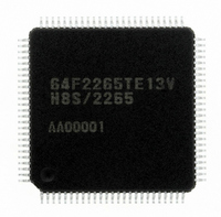
IC H8S/2265 MCU FLASH 100TQFP
Manufacturer
Renesas Electronics America
Series
H8® H8S/2200r
Specifications of DF2265TE13V
Core Processor
H8S/2000
Core Size
16-Bit
Speed
13MHz
Connectivity
I²C, SCI, SmartCard
Peripherals
LCD, POR, PWM, WDT
Number Of I /o
67
Program Memory Size
128KB (128K x 8)
Program Memory Type
FLASH
Ram Size
4K x 8
Voltage - Supply (vcc/vdd)
3 V ~ 5.5 V
Data Converters
A/D 10x10b, D/A 2x8b
Oscillator Type
Internal
Operating Temperature
-20°C ~ 75°C
Package / Case
100-TQFP, 100-VQFP
Lead Free Status / RoHS Status
Lead free / RoHS Compliant
Eeprom Size
-
Available stocks
Company
Part Number
Manufacturer
Quantity
Price
Company:

Part Number:
DF2265TE13V
Manufacturer:
Renesas Electronics America
Quantity:
10 000


Section 20 ROM
Do not apply a constant high level to the FWE pin: Apply a high level to the FWE pin only
when programming or erasing flash memory. A system configuration in which a high level is
constantly applied to the FWE pin should be avoided. Also, while a high level is applied to the
FWE pin, the watchdog timer should be activated to prevent overprogramming or overerasing due
to program runaway, etc.
Use the recommended algorithm when programming and erasing flash memory: The
recommended algorithm enables programming and erasing to be carried out without subjecting the
device to voltage stress or sacrificing program data reliability. When setting the P1 or E1 bit in
FLMCR1, the watchdog timer should be set beforehand as a precaution against program runaway,
etc.
Do not set or clear the SWE1 bit during execution of a program in flash memory: Wait for at
least 100 µs after clearing the SWE1 bit before executing a program or reading data in flash
memory.
When the SWE1 bit is set, data in flash memory can be rewritten. Access flash memory only for
verify operations (verification during programming/erasing). Also, do not clear the SWE1 bit
during programming, erasing, or verifying. Similarly, when using the RAM emulation function
while a high level is being input to the FWE pin, the SWE1 bit must be cleared before executing a
program or reading data in flash memory.
However, the RAM area overlapping flash memory space can be read and written to regardless of
whether the SWE1 bit is set or cleared.
Do not use interrupts while flash memory is being programmed or erased: All interrupt
requests, including NMI, should be disabled during FWE application to give priority to
program/erase operations.
Do not perform additional programming. Erase the memory before reprogramming: In on-
board programming, perform only one programming operation on a 128-byte programming unit
block. In programmer mode, too, perform only one programming operation on a 128-byte
programming unit block. Programming should be carried out with the entire programming unit
block erased.
Before programming, check that the chip is correctly mounted in the PROM programmer:
Overcurrent damage to the device can result if the index marks on the PROM programmer socket,
socket adapter, and chip are not correctly aligned.
Rev. 5.00 Sep. 01, 2009 Page 534 of 656
REJ09B0071-0500
Related parts for DF2265TE13V
Image
Part Number
Description
Manufacturer
Datasheet
Request
R

Part Number:
Description:
CONN SOCKET 2POS 7.92MM WHITE
Manufacturer:
Hirose Electric Co Ltd
Datasheet:

Part Number:
Description:
CONN SOCKET 4POS 7.92MM WHITE
Manufacturer:
Hirose Electric Co Ltd
Datasheet:

Part Number:
Description:
CONN SOCKET 5POS 7.92MM WHITE
Manufacturer:
Hirose Electric Co Ltd
Datasheet:

Part Number:
Description:
CONN SOCKET 3POS 7.92MM WHITE
Manufacturer:
Hirose Electric Co Ltd
Datasheet:
Part Number:
Description:
CONN SOCKET 5POS 7.92MM WHITE
Manufacturer:
Hirose Electric Co Ltd
Datasheet:

Part Number:
Description:
CONN SOCKET 2POS 7.92MM WHITE
Manufacturer:
Hirose Electric Co Ltd
Datasheet:
Part Number:
Description:
CONN SOCKET 3POS 7.92MM WHITE
Manufacturer:
Hirose Electric Co Ltd
Datasheet:
Part Number:
Description:
CONN SOCKET 4POS 7.92MM WHITE
Manufacturer:
Hirose Electric Co Ltd
Datasheet:

Part Number:
Description:
CONN HEADER 2POS 7.92MM R/A TIN
Manufacturer:
Hirose Electric Co Ltd
Datasheet:

Part Number:
Description:
CONN HEADER 4POS 7.92MM R/A TIN
Manufacturer:
Hirose Electric Co Ltd
Datasheet:

Part Number:
Description:
KIT STARTER FOR M16C/29
Manufacturer:
Renesas Electronics America
Datasheet:

Part Number:
Description:
KIT STARTER FOR R8C/2D
Manufacturer:
Renesas Electronics America
Datasheet:

Part Number:
Description:
R0K33062P STARTER KIT
Manufacturer:
Renesas Electronics America
Datasheet:

Part Number:
Description:
KIT STARTER FOR R8C/23 E8A
Manufacturer:
Renesas Electronics America
Datasheet:

Part Number:
Description:
KIT STARTER FOR R8C/25
Manufacturer:
Renesas Electronics America
Datasheet: