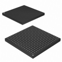
AT91SAM9G45-CU-999 Atmel, AT91SAM9G45-CU-999 Datasheet - Page 57

AT91SAM9G45-CU-999
Manufacturer Part Number
AT91SAM9G45-CU-999
Description
IC MCU ARM9 APMC 324TFBGA
Manufacturer
Atmel
Series
AT91SAMr
Datasheet
1.AT91SAM9G45-EKES.pdf
(1218 pages)
Specifications of AT91SAM9G45-CU-999
Core Processor
ARM9
Core Size
16/32-Bit
Speed
400MHz
Connectivity
EBI/EMI, Ethernet, I²C, IrDA, MMC, SPI, SSC, UART/USART, USB
Peripherals
AC'97, DMA, I²S, LCD, POR, PWM, WDT
Number Of I /o
160
Program Memory Size
64KB (64K x 8)
Program Memory Type
ROM
Ram Size
128K x 8
Voltage - Supply (vcc/vdd)
0.9 V ~ 1.1 V
Data Converters
A/D 8x10b
Oscillator Type
Internal
Operating Temperature
-40°C ~ 85°C
Package / Case
324-TFBGA
Lead Free Status / RoHS Status
Lead free / RoHS Compliant
Eeprom Size
-
Lead Free Status / Rohs Status
Supplier Unconfirmed
Available stocks
Company
Part Number
Manufacturer
Quantity
Price
- Current page: 57 of 1218
- Download datasheet (19Mb)
11. Boot Strategies
11.1
6438F–ATARM–21-Jun-10
Boot Program
The system always boots at address 0x0. To ensure maximum boot possibilities the memory
layout can be changed with two parameters.
Note: All the memory blocks can always be seen at their specified base addresses that are not
concerned by these parameters.
The AT91SAM9G45 manages a boot memory that depends on the level on the BMS pin at
reset. The internal memory area mapped between address 0x0 and 0x000F FFFF is reserved to
this effect.
If BMS is detected at 0, the boot memory is the memory connected on the Chip Select 0 of the
External Bus Interface.
For optimization purpose, nothing else is done. To speed up the boot sequence user pro-
grammed software should perform a complete configuration:
If BMS is detected at 1, the boot memory is the embedded ROM and the boot program
described below is executed.
The Boot Program is contained in the embedded ROM. It is also called: “Rom Code” or “First
level bootloader”. At power on, if the BMS pin is detected at 1, the boot memory is the embed-
ded ROM and the Boot Program is executed.
The Boot Program consists of several steps. First, it performs device initialization. Then it
attempts to boot from external non volatile memories (NVM). And finally, if no valid program is
found in NVM, it executes a monitor called SAM-BA
• REMAP allows the user to layout the internal SRAM bank to 0x0 to ease the development.
• BMS allows the user to layout to 0x0, when convenient, the ROM or an external memory. This
• Boot on on-chip RC
• Boot with the default configuration for the Static Memory Controller, byte select mode, 16-bit
• Enable the 32768 Hz oscillator if best accuracy is needed
• Program the PMC (main oscillator enable or bypass mode)
• Program and Start the PLL
• Reprogram the SMC setup, cycle, hold, mode timings registers for EBI CS0 to adapt them to
• Switch the system clock to the new value
This is done by software once the system has boot.
is done by hardware at reset.
data bus, Read/Write controlled by Chip Select, allows boot on 16-bit non-volatile memory.
the new clock
®
Monitor.
AT91SAM9G45
57
Related parts for AT91SAM9G45-CU-999
Image
Part Number
Description
Manufacturer
Datasheet
Request
R

Part Number:
Description:
KIT EVAL FOR AT91SAM9G45
Manufacturer:
Atmel
Datasheet:

Part Number:
Description:
MCU ARM9 324-TFBGA
Manufacturer:
Atmel
Datasheet:

Part Number:
Description:
At91 Arm Thumb-based Microcontrollers
Manufacturer:
ATMEL Corporation
Datasheet:

Part Number:
Description:
MCU, MPU & DSP Development Tools KICKSTART KIT FOR AT91SAM9 PLUS
Manufacturer:
IAR Systems

Part Number:
Description:
DEV KIT FOR AVR/AVR32
Manufacturer:
Atmel
Datasheet:

Part Number:
Description:
INTERVAL AND WIPE/WASH WIPER CONTROL IC WITH DELAY
Manufacturer:
ATMEL Corporation
Datasheet:

Part Number:
Description:
Low-Voltage Voice-Switched IC for Hands-Free Operation
Manufacturer:
ATMEL Corporation
Datasheet:

Part Number:
Description:
MONOLITHIC INTEGRATED FEATUREPHONE CIRCUIT
Manufacturer:
ATMEL Corporation
Datasheet:

Part Number:
Description:
AM-FM Receiver IC U4255BM-M
Manufacturer:
ATMEL Corporation
Datasheet:

Part Number:
Description:
Monolithic Integrated Feature Phone Circuit
Manufacturer:
ATMEL Corporation
Datasheet:

Part Number:
Description:
Multistandard Video-IF and Quasi Parallel Sound Processing
Manufacturer:
ATMEL Corporation
Datasheet:

Part Number:
Description:
High-performance EE PLD
Manufacturer:
ATMEL Corporation
Datasheet:


