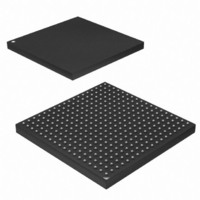
AT91SAM9G45-CU-999 Atmel, AT91SAM9G45-CU-999 Datasheet - Page 236

AT91SAM9G45-CU-999
Manufacturer Part Number
AT91SAM9G45-CU-999
Description
IC MCU ARM9 APMC 324TFBGA
Manufacturer
Atmel
Series
AT91SAMr
Datasheet
1.AT91SAM9G45-EKES.pdf
(1218 pages)
Specifications of AT91SAM9G45-CU-999
Core Processor
ARM9
Core Size
16/32-Bit
Speed
400MHz
Connectivity
EBI/EMI, Ethernet, I²C, IrDA, MMC, SPI, SSC, UART/USART, USB
Peripherals
AC'97, DMA, I²S, LCD, POR, PWM, WDT
Number Of I /o
160
Program Memory Size
64KB (64K x 8)
Program Memory Type
ROM
Ram Size
128K x 8
Voltage - Supply (vcc/vdd)
0.9 V ~ 1.1 V
Data Converters
A/D 8x10b
Oscillator Type
Internal
Operating Temperature
-40°C ~ 85°C
Package / Case
324-TFBGA
Lead Free Status / RoHS Status
Lead free / RoHS Compliant
Eeprom Size
-
Lead Free Status / Rohs Status
Supplier Unconfirmed
Available stocks
Company
Part Number
Manufacturer
Quantity
Price
- Current page: 236 of 1218
- Download datasheet (19Mb)
22.4
22.4.1
236
Functional Description
AT91SAM9G45
SDRAM Controller Write Cycle
The DDRSDRC allows burst access or single access in normal mode (mode = 000). Whatever
the access type, the DDRSDRC keeps track of the active row in each bank, thus maximizing
performance.
The SDRAM device is programmed with a burst length equal to 8. This determines the length of
a sequential data input by the write command that is set to 8. The latency from write command to
data input is fixed to 1 in the case of DDR-SDRAM devices. In the case of SDR-SDRAM
devices, there is no latency from write command to data input.
To initiate a single access, the DDRSDRC checks if the page access is already open. If
row/bank addresses match with the previous row/bank addresses, the controller generates a
write command. If the bank addresses are not identical or if bank addresses are identical but the
row addresses are not identical, the controller generates a precharge command, activates the
new row and initiates a write command. To comply with SDRAM timing parameters, additional
clock cycles are inserted between precharge/active (t RP) commands and active/write (t RCD)
command. As the burst length is fixed to 8, in the case of single access, it has to stop the burst,
otherwise seven invalid values may be written. In the case of SDR-SDRAM devices, a Burst
Stop command is generated to interrupt the write operation. In the case of DDR-SDRAM
devices, Burst Stop command is not supported for the burst write operation. In order to then
interrupt the write operation, Dm must be set to 1 to mask invalid data (see
237
To initiate a burst access, the DDRSDRC uses the transfer type signal provided by the master
requesting the access. If the next access is a sequential write access, writing to the SDRAM
device is carried out. If the next access is a write non-sequential access, then an automatic
access break is inserted, the DDRSDRC generates a precharge command, activates the new
row and initiates a write command. To comply with SDRAM timing parameters, additional clock
cycles are inserted between precharge/active (tRP) commands and active/write (tRCD)
commands.
For a definition of timing parameters, refer to
Register” on page
Write accesses to the SDRAM devices are burst oriented and the burst length is programmed to
8. It determines the maximum number of column locations that can be accessed for a given write
command. When the write command is issued, 8 columns are selected. All accesses for that
burst take place within these eight columns, thus the burst wraps within these 8 columns if a
boundary is reached. These 8 columns are selected by addr[13:3]. addr[2:0] is used to select the
starting location within the block.
In the case of incrementing burst (INCR/INCR4/INCR8/INCR16), the addresses can cross the
16-byte boundary of the SDRAM device. For example, in the case of DDR-SDRAM devices,
when a transfer (INCR4) starts at address 0x0C, the next access is 0x10, but since the burst
length is programmed to 8, the next access is at 0x00. Since the boundary is reached, the burst
is wrapping. The DDRSDRC takes this feature of the SDRAM device into account. In the case of
transfer starting at address 0x04/0x08/0x0C (DDR-SDRAM devices) or starting at address
0x10/0x14/0x18/0x1C, two write commands are issued to avoid to wrap when the boundary is
reached. The last write command is subject to DM input logic level. If DM is registered high, the
corresponding data input is ignored and write access is not done. This avoids additional writing
being done.
and
Figure 22-5 on page
265.
238) and DQS must continue to toggle.
Section 22.7.4 “DDRSDRC Timing 0 Parameter
Figure 22-2 on page
6438F–ATARM–21-Jun-10
Related parts for AT91SAM9G45-CU-999
Image
Part Number
Description
Manufacturer
Datasheet
Request
R

Part Number:
Description:
KIT EVAL FOR AT91SAM9G45
Manufacturer:
Atmel
Datasheet:

Part Number:
Description:
MCU ARM9 324-TFBGA
Manufacturer:
Atmel
Datasheet:

Part Number:
Description:
At91 Arm Thumb-based Microcontrollers
Manufacturer:
ATMEL Corporation
Datasheet:

Part Number:
Description:
MCU, MPU & DSP Development Tools KICKSTART KIT FOR AT91SAM9 PLUS
Manufacturer:
IAR Systems

Part Number:
Description:
DEV KIT FOR AVR/AVR32
Manufacturer:
Atmel
Datasheet:

Part Number:
Description:
INTERVAL AND WIPE/WASH WIPER CONTROL IC WITH DELAY
Manufacturer:
ATMEL Corporation
Datasheet:

Part Number:
Description:
Low-Voltage Voice-Switched IC for Hands-Free Operation
Manufacturer:
ATMEL Corporation
Datasheet:

Part Number:
Description:
MONOLITHIC INTEGRATED FEATUREPHONE CIRCUIT
Manufacturer:
ATMEL Corporation
Datasheet:

Part Number:
Description:
AM-FM Receiver IC U4255BM-M
Manufacturer:
ATMEL Corporation
Datasheet:

Part Number:
Description:
Monolithic Integrated Feature Phone Circuit
Manufacturer:
ATMEL Corporation
Datasheet:

Part Number:
Description:
Multistandard Video-IF and Quasi Parallel Sound Processing
Manufacturer:
ATMEL Corporation
Datasheet:

Part Number:
Description:
High-performance EE PLD
Manufacturer:
ATMEL Corporation
Datasheet:


