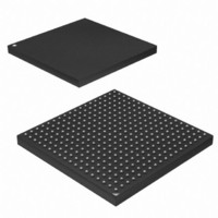
AT91SAM9G45-CU-999 Atmel, AT91SAM9G45-CU-999 Datasheet - Page 1099

AT91SAM9G45-CU-999
Manufacturer Part Number
AT91SAM9G45-CU-999
Description
IC MCU ARM9 APMC 324TFBGA
Manufacturer
Atmel
Series
AT91SAMr
Datasheet
1.AT91SAM9G45-EKES.pdf
(1218 pages)
Specifications of AT91SAM9G45-CU-999
Core Processor
ARM9
Core Size
16/32-Bit
Speed
400MHz
Connectivity
EBI/EMI, Ethernet, I²C, IrDA, MMC, SPI, SSC, UART/USART, USB
Peripherals
AC'97, DMA, I²S, LCD, POR, PWM, WDT
Number Of I /o
160
Program Memory Size
64KB (64K x 8)
Program Memory Type
ROM
Ram Size
128K x 8
Voltage - Supply (vcc/vdd)
0.9 V ~ 1.1 V
Data Converters
A/D 8x10b
Oscillator Type
Internal
Operating Temperature
-40°C ~ 85°C
Package / Case
324-TFBGA
Lead Free Status / RoHS Status
Lead free / RoHS Compliant
Eeprom Size
-
Lead Free Status / Rohs Status
Supplier Unconfirmed
Available stocks
Company
Part Number
Manufacturer
Quantity
Price
- Current page: 1099 of 1218
- Download datasheet (19Mb)
45.5.3
45.6
45.6.1
45.6.1.1
45.6.1.2
45.6.1.3
6438F–ATARM–21-Jun-10
Functional Description
Interrupt Sources
DMA Controller
Configuration Block
AHB Interface
Channel-U
The LCD Controller interrupt line is connected to one of the internal sources of the Advanced
Interrupt Controller. Using the LCD Controller interrupt requires prior programming of the AIC.
Table 45-3.
The LCD Controller consists of two main blocks
and the LCD controller core (LCDC core). The DMA controller reads the display data from an
external memory through a AHB master interface. The LCD controller core formats the display
data. The LCD controller core continuously pumps the pixel data into the LCD module via the
LCD data bus (LCDD[23:0]); this bus is timed by the LCDDOTCK, LCDDEN, LCDHSYNC, and
LCDVSYNC signals.
The configuration block is a set of programmable registers that are used to configure the DMA
controller operation. These registers are written via the AHB slave interface. Only word access is
allowed.
For details on the configuration registers, see
1125.
This block generates the AHB transactions. It generates undefined-length incrementing bursts
as well as 4-, 8- or 16-beat incrementing bursts. The size of the transfer can be configured in the
BRSTLN field of the DMAFRMCFG register. For details on this register, see
figuration Register” on page
This block stores the base address and the number of words transferred for this channel (frame
in single scan mode and Upper Panel in dual scan mode) since the beginning of the frame. It
also generates the end of frame signal.
It has two pointers, the base address and the number of words to transfer. When the module
receives a new_frame signal, it reloads the number of words to transfer pointer with the size of
the frame/panel. When the module receives the new_frame signal, it also reloads the base
address with the base address programmed by the host.
The size of the frame/panel can be programmed in the FRMSIZE field of the DMAFRMCFG
Register. This size is calculated as follows:
where:
X_size = ((LINESIZE+1)*Bpp+PIXELOFF)/32
Y_size = (LINEVAL+1)
Instance
LCDC
Peripheral IDs
Frame_size
23
ID
1130.
=
X_size*Y_size
------------------------------------- -
32
“LCD Controller (LCDC) User Interface” on page
(Figure 45-1 on page
AT91SAM9G45
1096), the DMA controller
“DMA Frame Con-
1099
Related parts for AT91SAM9G45-CU-999
Image
Part Number
Description
Manufacturer
Datasheet
Request
R

Part Number:
Description:
KIT EVAL FOR AT91SAM9G45
Manufacturer:
Atmel
Datasheet:

Part Number:
Description:
MCU ARM9 324-TFBGA
Manufacturer:
Atmel
Datasheet:

Part Number:
Description:
At91 Arm Thumb-based Microcontrollers
Manufacturer:
ATMEL Corporation
Datasheet:

Part Number:
Description:
MCU, MPU & DSP Development Tools KICKSTART KIT FOR AT91SAM9 PLUS
Manufacturer:
IAR Systems

Part Number:
Description:
DEV KIT FOR AVR/AVR32
Manufacturer:
Atmel
Datasheet:

Part Number:
Description:
INTERVAL AND WIPE/WASH WIPER CONTROL IC WITH DELAY
Manufacturer:
ATMEL Corporation
Datasheet:

Part Number:
Description:
Low-Voltage Voice-Switched IC for Hands-Free Operation
Manufacturer:
ATMEL Corporation
Datasheet:

Part Number:
Description:
MONOLITHIC INTEGRATED FEATUREPHONE CIRCUIT
Manufacturer:
ATMEL Corporation
Datasheet:

Part Number:
Description:
AM-FM Receiver IC U4255BM-M
Manufacturer:
ATMEL Corporation
Datasheet:

Part Number:
Description:
Monolithic Integrated Feature Phone Circuit
Manufacturer:
ATMEL Corporation
Datasheet:

Part Number:
Description:
Multistandard Video-IF and Quasi Parallel Sound Processing
Manufacturer:
ATMEL Corporation
Datasheet:

Part Number:
Description:
High-performance EE PLD
Manufacturer:
ATMEL Corporation
Datasheet:


