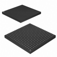
AT91SAM9G45-CU-999 Atmel, AT91SAM9G45-CU-999 Datasheet - Page 421

AT91SAM9G45-CU-999
Manufacturer Part Number
AT91SAM9G45-CU-999
Description
IC MCU ARM9 APMC 324TFBGA
Manufacturer
Atmel
Series
AT91SAMr
Datasheet
1.AT91SAM9G45-EKES.pdf
(1218 pages)
Specifications of AT91SAM9G45-CU-999
Core Processor
ARM9
Core Size
16/32-Bit
Speed
400MHz
Connectivity
EBI/EMI, Ethernet, I²C, IrDA, MMC, SPI, SSC, UART/USART, USB
Peripherals
AC'97, DMA, I²S, LCD, POR, PWM, WDT
Number Of I /o
160
Program Memory Size
64KB (64K x 8)
Program Memory Type
ROM
Ram Size
128K x 8
Voltage - Supply (vcc/vdd)
0.9 V ~ 1.1 V
Data Converters
A/D 8x10b
Oscillator Type
Internal
Operating Temperature
-40°C ~ 85°C
Package / Case
324-TFBGA
Lead Free Status / RoHS Status
Lead free / RoHS Compliant
Eeprom Size
-
Lead Free Status / Rohs Status
Supplier Unconfirmed
Available stocks
Company
Part Number
Manufacturer
Quantity
Price
- Current page: 421 of 1218
- Download datasheet (19Mb)
29. Serial Peripheral Interface (SPI)
29.1
29.2
6438F–ATARM–21-Jun-10
Description
Embedded Characteristics
The Serial Peripheral Interface (SPI) circuit is a synchronous serial data link that provides com-
munication with external devices in Master or Slave Mode. It also enables communication
between processors if an external processor is connected to the system.
The Serial Peripheral Interface is essentially a shift register that serially transmits data bits to
other SPIs. During a data transfer, one SPI system acts as the “master”' which controls the data
flow, while the other devices act as “slaves'' which have data shifted into and out by the master.
Different CPUs can take turn being masters (Multiple Master Protocol opposite to Single Master
Protocol where one CPU is always the master while all of the others are always slaves) and one
master may simultaneously shift data into multiple slaves. However, only one slave may drive its
output to write data back to the master at any given time.
A slave device is selected when the master asserts its NSS signal. If multiple slave devices
exist, the master generates a separate slave select signal for each slave (NPCS).
The SPI system consists of two data lines and two control lines:
• Master Out Slave In (MOSI): This data line supplies the output data from the master shifted
• Master In Slave Out (MISO): This data line supplies the output data from a slave to the input
• Serial Clock (SPCK): This control line is driven by the master and regulates the flow of the
• Slave Select (NSS): This control line allows slaves to be turned on and off by hardware.
• Supports communication with serial external devices
• Master or slave serial peripheral bus interface
• Very fast transfers supported
into the input(s) of the slave(s).
of the master. There may be no more than one slave transmitting data during any particular
transfer.
data bits. The master may transmit data at a variety of baud rates; the SPCK line cycles once
for each bit that is transmitted.
– Four chip selects with external decoder support allow communication with up to 15
– Serial memories, such as DataFlash and 3-wire EEPROMs
– Serial peripherals, such as ADCs, DACs, LCD Controllers, CAN Controllers and
– External co-processors
– 8- to 16-bit programmable data length per chip select
– Programmable phase and polarity per chip select
– Programmable transfer delays between consecutive transfers and between clock
– Programmable delay between consecutive transfers
– Selectable mode fault detection
– Transfers with baud rates up to MCK
– The chip select line may be left active to speed up transfers on the same device
peripherals
Sensors
and data per chip select
AT91SAM9G45
421
Related parts for AT91SAM9G45-CU-999
Image
Part Number
Description
Manufacturer
Datasheet
Request
R

Part Number:
Description:
KIT EVAL FOR AT91SAM9G45
Manufacturer:
Atmel
Datasheet:

Part Number:
Description:
MCU ARM9 324-TFBGA
Manufacturer:
Atmel
Datasheet:

Part Number:
Description:
At91 Arm Thumb-based Microcontrollers
Manufacturer:
ATMEL Corporation
Datasheet:

Part Number:
Description:
MCU, MPU & DSP Development Tools KICKSTART KIT FOR AT91SAM9 PLUS
Manufacturer:
IAR Systems

Part Number:
Description:
DEV KIT FOR AVR/AVR32
Manufacturer:
Atmel
Datasheet:

Part Number:
Description:
INTERVAL AND WIPE/WASH WIPER CONTROL IC WITH DELAY
Manufacturer:
ATMEL Corporation
Datasheet:

Part Number:
Description:
Low-Voltage Voice-Switched IC for Hands-Free Operation
Manufacturer:
ATMEL Corporation
Datasheet:

Part Number:
Description:
MONOLITHIC INTEGRATED FEATUREPHONE CIRCUIT
Manufacturer:
ATMEL Corporation
Datasheet:

Part Number:
Description:
AM-FM Receiver IC U4255BM-M
Manufacturer:
ATMEL Corporation
Datasheet:

Part Number:
Description:
Monolithic Integrated Feature Phone Circuit
Manufacturer:
ATMEL Corporation
Datasheet:

Part Number:
Description:
Multistandard Video-IF and Quasi Parallel Sound Processing
Manufacturer:
ATMEL Corporation
Datasheet:

Part Number:
Description:
High-performance EE PLD
Manufacturer:
ATMEL Corporation
Datasheet:


