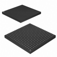
AT91SAM9G45-CU-999 Atmel, AT91SAM9G45-CU-999 Datasheet - Page 1132

AT91SAM9G45-CU-999
Manufacturer Part Number
AT91SAM9G45-CU-999
Description
IC MCU ARM9 APMC 324TFBGA
Manufacturer
Atmel
Series
AT91SAMr
Datasheet
1.AT91SAM9G45-EKES.pdf
(1218 pages)
Specifications of AT91SAM9G45-CU-999
Core Processor
ARM9
Core Size
16/32-Bit
Speed
400MHz
Connectivity
EBI/EMI, Ethernet, I²C, IrDA, MMC, SPI, SSC, UART/USART, USB
Peripherals
AC'97, DMA, I²S, LCD, POR, PWM, WDT
Number Of I /o
160
Program Memory Size
64KB (64K x 8)
Program Memory Type
ROM
Ram Size
128K x 8
Voltage - Supply (vcc/vdd)
0.9 V ~ 1.1 V
Data Converters
A/D 8x10b
Oscillator Type
Internal
Operating Temperature
-40°C ~ 85°C
Package / Case
324-TFBGA
Lead Free Status / RoHS Status
Lead free / RoHS Compliant
Eeprom Size
-
Lead Free Status / Rohs Status
Supplier Unconfirmed
Available stocks
Company
Part Number
Manufacturer
Quantity
Price
- Current page: 1132 of 1218
- Download datasheet (19Mb)
45.12.9
Name: DMA2DCFG
Address:0x00500020
Access: Read-write
Reset value: 0x00000000
• ADDRINC: DMA 2D Addressing Address increment
When 2-D DMA addressing is enabled (bit DMA2DEN is set in register DMACON), this field specifies the number of bytes
that the DMA controller must jump between screen lines. Itb must be programmed as: [({address of first 32-bit word in a
screen line} - {address of last 32-bit word in previous line})]. In other words, it is equal to 4*[number of 32-bit words occu-
pied by each line in the complete frame buffer minus the number of 32-bit words occupied by each displayed line]. Bit
DMAUPDT in register DMACON must be written after writing any new value to this field in order to make the DMA control-
ler use this new value.
• PIXELOFF: DAM2D Addressing Pixel offset
When 2D DMA addressing is enabled (bit DMA2DEN is set in register DMACON), this field specifies the offset of the first
pixel in each line within the memory word that contains this pixel. The offset is specified in number of bits in the range 0-31,
so for example a value of 4 indicates that the first pixel in the screen starts at bit 4 of the 32-bit word pointed by register
DMABADDR1. Bits 0 to 3 of that word are not used. This example is valid for little endian memory organization. When
using big endian memory organization, this offset is considered from bit 31 downwards, or equivalently, a given value of
this field always selects the pixel in the same relative position within the word, independently of the memory ordering con-
figuration. Bit DMAUPDT in register DMACON must be written after writing any new value to this field in order to make the
DMA controller use this new value.
1132
31
23
15
–
–
7
AT91SAM9G45
LCD DMA 2D Addressing Register
30
22
14
–
–
6
29
21
13
–
–
5
28
20
12
–
4
ADDRINC
ADDRINC
27
19
11
–
3
PIXELOFF
26
18
10
–
2
25
17
–
9
1
6438F–ATARM–21-Jun-10
24
16
–
8
0
Related parts for AT91SAM9G45-CU-999
Image
Part Number
Description
Manufacturer
Datasheet
Request
R

Part Number:
Description:
KIT EVAL FOR AT91SAM9G45
Manufacturer:
Atmel
Datasheet:

Part Number:
Description:
MCU ARM9 324-TFBGA
Manufacturer:
Atmel
Datasheet:

Part Number:
Description:
At91 Arm Thumb-based Microcontrollers
Manufacturer:
ATMEL Corporation
Datasheet:

Part Number:
Description:
MCU, MPU & DSP Development Tools KICKSTART KIT FOR AT91SAM9 PLUS
Manufacturer:
IAR Systems

Part Number:
Description:
DEV KIT FOR AVR/AVR32
Manufacturer:
Atmel
Datasheet:

Part Number:
Description:
INTERVAL AND WIPE/WASH WIPER CONTROL IC WITH DELAY
Manufacturer:
ATMEL Corporation
Datasheet:

Part Number:
Description:
Low-Voltage Voice-Switched IC for Hands-Free Operation
Manufacturer:
ATMEL Corporation
Datasheet:

Part Number:
Description:
MONOLITHIC INTEGRATED FEATUREPHONE CIRCUIT
Manufacturer:
ATMEL Corporation
Datasheet:

Part Number:
Description:
AM-FM Receiver IC U4255BM-M
Manufacturer:
ATMEL Corporation
Datasheet:

Part Number:
Description:
Monolithic Integrated Feature Phone Circuit
Manufacturer:
ATMEL Corporation
Datasheet:

Part Number:
Description:
Multistandard Video-IF and Quasi Parallel Sound Processing
Manufacturer:
ATMEL Corporation
Datasheet:

Part Number:
Description:
High-performance EE PLD
Manufacturer:
ATMEL Corporation
Datasheet:


