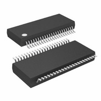
ATMEGA32HVB-8X3 Atmel, ATMEGA32HVB-8X3 Datasheet - Page 75

ATMEGA32HVB-8X3
Manufacturer Part Number
ATMEGA32HVB-8X3
Description
MCU AVR 32KB FLASH 8MHZ 44TSSOP
Manufacturer
Atmel
Series
AVR® ATmegar
Specifications of ATMEGA32HVB-8X3
Core Processor
AVR
Core Size
8-Bit
Speed
8MHz
Connectivity
I²C, SPI
Peripherals
POR, WDT
Number Of I /o
17
Program Memory Size
32KB (16K x 16)
Program Memory Type
FLASH
Eeprom Size
1K x 8
Ram Size
2K x 8
Voltage - Supply (vcc/vdd)
4 V ~ 25 V
Data Converters
A/D 7x12b
Oscillator Type
External
Operating Temperature
-40°C ~ 85°C
Package / Case
44-TSSOP
Processor Series
ATMEGA32x
Core
AVR8
Data Bus Width
8 bit
Data Ram Size
2 KB
Interface Type
SPI, TWI
Maximum Clock Frequency
8 MHz
Number Of Programmable I/os
17
Number Of Timers
2
Maximum Operating Temperature
+ 85 C
Mounting Style
SMD/SMT
Development Tools By Supplier
ATAVRDRAGON, ATSTK500, ATSTK600, ATAVRISP2, ATAVRONEKIT, ATAVRSB200
Minimum Operating Temperature
- 40 C
On-chip Adc
12 bit, 7 Channel
Package
44TSSOP
Device Core
AVR
Family Name
ATmega
Maximum Speed
8 MHz
Operating Supply Voltage
5|9|12|15|18|24 V
For Use With
ATSTK524 - KIT STARTER ATMEGA32M1/MEGA32C1ATSTK600 - DEV KIT FOR AVR/AVR32ATAVRDRAGON - KIT DRAGON 32KB FLASH MEM AVRATSTK500 - PROGRAMMER AVR STARTER KIT
Lead Free Status / RoHS Status
Lead free / RoHS Compliant
Available stocks
Company
Part Number
Manufacturer
Quantity
Price
Company:
Part Number:
ATMEGA32HVB-8X3
Manufacturer:
Atmel
Quantity:
408
- Current page: 75 of 275
- Download datasheet (7Mb)
Table 15-4.
15.3.2
8042B–AVR–06/10
Signal Name
PUOE
PUOV
DDOE
DDOV
PVOE
PVOV
PTOE
DIEOE
DIEOV
DI
AIO
Alternate Functions of Port B
Overriding Signals for Alternate Functions in PA3:PA0
PA3/T1/PCINT3
PCINT3 • PCIE0
PCINT3 INPUT
T1 INPUT
These pins can serve as external interrupt
Port A to the overriding signals shown in
The Port B pins with alternate functions are shown in
Table 15-5.
The alternate pin configuration is as follows:
• MISO/PCINT11 – Port B, Bit7
MISO, Master Data input: Slave Data output pin for SPI channel. When the SPI is enabled as a
Master, this pin is configured as an input regardless of the setting of DDB7. When the SPI is
enabled as a Slave, the data direction of this pin is controlled by DDB7. When the pin is forced
by the SPI to be an input, the pull-up can still be controlled by the PORTB7 bit. When not operat-
ing in SPI mode, this pin can serve as an external interrupt source.
PCINT11: Pin Change Interrupt 11. This pin can serve as external interrupt source.
0
0
0
0
0
0
1
-
-
Port Pin
PB7
PB6
PB5
PB4
PB3
PB2
PB1
PB0
Alternate Functions
MISO/PCINT11 (SPI Bus Master Input/Slave Output or Pin Change Interrupt 11)
MOSI/PCINT10 (SPI Bus Master Output/Slave Input or Pin Change Interrupt 10)
SCK/PCINT9 (SPI Bus Serial Clock or Pin Change Interrupt 9)
SS/PCINT8 (SPI Bus Slave Select input or Pin Change Interrupt 8)
PCINT7 (Pin Change Interrupt 7)
PCINT6 (Pin Change Interrupt 6)
CKOUT/PCINT5 (Clock output or Pin Change Interrupt 5)
PCINT4/ICP00 (Pin Change Interrupt 4
Port B Pins Alternate Functions
PA2/T0/PCINT2
PCINT2 • PCIE0
PCINT2 INPUT
T0 INPUT
0
0
0
0
0
0
1
-
-
PA1/ADC1/SGND/PCINT1
Figure 15-5 on page
VADSC • VADMUX=ADC0
VADSC • VADMUX=ADC0
DIDR1| (PCINT1 • PCIE0)
ADC1 INPUT/ SGND
sourceTable 15-4
PCINT1 INPUT
or Timer/Counter0 Input Capture Trigger
DIDR1
ATmega16HVB/32HVB
0
0
1
0
-
Table
15-5.
72.
relates the alternate functions of
PA0/ADC0/SGND/PCINT0
VADSC • VADMUX=ADC1
VADSC • VADMUX=ADC1
DIDR0 | (PCINT0 • PCIE0)
ADC0 INPUT/ SGND
PCINT0 INPUT
DIDR0
0
0
1
0
-
)
75
Related parts for ATMEGA32HVB-8X3
Image
Part Number
Description
Manufacturer
Datasheet
Request
R

Part Number:
Description:
Manufacturer:
Atmel Corporation
Datasheet:

Part Number:
Description:
Manufacturer:
ATMEL Corporation
Datasheet:

Part Number:
Description:
IC AVR MCU 32K 16MHZ 5V 44-QFN
Manufacturer:
Atmel
Datasheet:

Part Number:
Description:
IC AVR MCU 32K 16MHZ 5V 40DIP
Manufacturer:
Atmel
Datasheet:

Part Number:
Description:
IC AVR MCU 32K 16MHZ 5V 44TQFP
Manufacturer:
Atmel
Datasheet:

Part Number:
Description:
IC AVR MCU 32K 16MHZ IND 40-DIP
Manufacturer:
Atmel
Datasheet:

Part Number:
Description:
IC AVR MCU 32K 16MHZ IND 44-TQFP
Manufacturer:
Atmel
Datasheet:

Part Number:
Description:
MCU AVR 32KB FLASH 16MHZ 44TQFP
Manufacturer:
Atmel
Datasheet:

Part Number:
Description:
MCU AVR 32KB FLASH 16MHZ 44QFN
Manufacturer:
Atmel
Datasheet:

Part Number:
Description:
MCU AVR 32K FLASH 16MHZ 44-TQFP
Manufacturer:
Atmel
Datasheet:

Part Number:
Description:
IC AVR MCU 32K 16MHZ COM 40-DIP
Manufacturer:
Atmel
Datasheet:

Part Number:
Description:
IC AVR MCU 32K 16MHZ COM 44-QFN
Manufacturer:
Atmel
Datasheet:

Part Number:
Description:
IC AVR MCU 32K 16MHZ COM 44-TQFP
Manufacturer:
Atmel
Datasheet:


