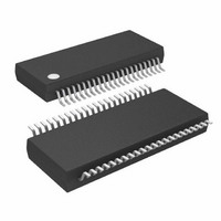
ATMEGA32HVB-8X3 Atmel, ATMEGA32HVB-8X3 Datasheet - Page 212

ATMEGA32HVB-8X3
Manufacturer Part Number
ATMEGA32HVB-8X3
Description
MCU AVR 32KB FLASH 8MHZ 44TSSOP
Manufacturer
Atmel
Series
AVR® ATmegar
Specifications of ATMEGA32HVB-8X3
Core Processor
AVR
Core Size
8-Bit
Speed
8MHz
Connectivity
I²C, SPI
Peripherals
POR, WDT
Number Of I /o
17
Program Memory Size
32KB (16K x 16)
Program Memory Type
FLASH
Eeprom Size
1K x 8
Ram Size
2K x 8
Voltage - Supply (vcc/vdd)
4 V ~ 25 V
Data Converters
A/D 7x12b
Oscillator Type
External
Operating Temperature
-40°C ~ 85°C
Package / Case
44-TSSOP
Processor Series
ATMEGA32x
Core
AVR8
Data Bus Width
8 bit
Data Ram Size
2 KB
Interface Type
SPI, TWI
Maximum Clock Frequency
8 MHz
Number Of Programmable I/os
17
Number Of Timers
2
Maximum Operating Temperature
+ 85 C
Mounting Style
SMD/SMT
Development Tools By Supplier
ATAVRDRAGON, ATSTK500, ATSTK600, ATAVRISP2, ATAVRONEKIT, ATAVRSB200
Minimum Operating Temperature
- 40 C
On-chip Adc
12 bit, 7 Channel
Package
44TSSOP
Device Core
AVR
Family Name
ATmega
Maximum Speed
8 MHz
Operating Supply Voltage
5|9|12|15|18|24 V
For Use With
ATSTK524 - KIT STARTER ATMEGA32M1/MEGA32C1ATSTK600 - DEV KIT FOR AVR/AVR32ATAVRDRAGON - KIT DRAGON 32KB FLASH MEM AVRATSTK500 - PROGRAMMER AVR STARTER KIT
Lead Free Status / RoHS Status
Lead free / RoHS Compliant
Available stocks
Company
Part Number
Manufacturer
Quantity
Price
Company:
Part Number:
ATMEGA32HVB-8X3
Manufacturer:
Atmel
Quantity:
408
- Current page: 212 of 275
- Download datasheet (7Mb)
30.6.1
8042B–AVR–06/10
Serial Programming Algorithm
Figure 30-1. Serial Programming and Verify.
Table 30-10. Pin Mapping Serial Programming
When programming the EEPROM, an auto-erase cycle is built into the self-timed programming
operation (in the Serial mode ONLY) and there is no need to first execute the Chip Erase
instruction. The Chip Erase operation turns the content of every memory location in both the
Program and EEPROM arrays into 0xFF.
Depending on OSCSEL Fuses, a valid clock must be present. The minimum low and high peri-
ods for the serial clock (SCK) input are defined as follows:
Low: > 2.2 CPU clock cycles for f
High: > 2.2 CPU clock cycles for f
When writing serial data to the ATmega16HVB/32HVB, data is clocked on the rising edge of
SCK.
When reading data from the ATmega16HVB/32HVB, data is clocked on the falling edge of SCK.
See
To program and verify the ATmega16HVB/32HVB in the Serial Programming mode, the follow-
ing sequence is recommended (see four byte instruction formats in
1. Power-up sequence:
Make sure the chip is started as explained in
ger Connect” on page 43
programmer can not guarantee that SCK is held low during power-up. In this case,
”Serial Programming Characteristics” on page 239
Symbol
MOSI
MISO
SCK
MOSI
MOSI
MISO
MISO
SCK
SCK
while RESET and SCK are set to “0”. In some systems, the
Pins
PB5
PB6
PB7
ck
ck
< 12 MHz, 3 CPU clock cycles for f
< 12 MHz, 3 CPU clock cycles for f
RESET
RESET
GND
GND
I/O
O
I
I
Section 11.2.1 ”Power-on Reset and Char-
ATmega16HVB/32HVB
for timing details.
V
V
FET
FET
+4.0 - 25.0V
+4.0 - 25.0V
Table 30-12 on page
Serial Data out
Serial Data in
Description
Serial Clock
ck
ck
>= 12 MHz
>= 12 MHz
214):
212
Related parts for ATMEGA32HVB-8X3
Image
Part Number
Description
Manufacturer
Datasheet
Request
R

Part Number:
Description:
Manufacturer:
Atmel Corporation
Datasheet:

Part Number:
Description:
Manufacturer:
ATMEL Corporation
Datasheet:

Part Number:
Description:
IC AVR MCU 32K 16MHZ 5V 44-QFN
Manufacturer:
Atmel
Datasheet:

Part Number:
Description:
IC AVR MCU 32K 16MHZ 5V 40DIP
Manufacturer:
Atmel
Datasheet:

Part Number:
Description:
IC AVR MCU 32K 16MHZ 5V 44TQFP
Manufacturer:
Atmel
Datasheet:

Part Number:
Description:
IC AVR MCU 32K 16MHZ IND 40-DIP
Manufacturer:
Atmel
Datasheet:

Part Number:
Description:
IC AVR MCU 32K 16MHZ IND 44-TQFP
Manufacturer:
Atmel
Datasheet:

Part Number:
Description:
MCU AVR 32KB FLASH 16MHZ 44TQFP
Manufacturer:
Atmel
Datasheet:

Part Number:
Description:
MCU AVR 32KB FLASH 16MHZ 44QFN
Manufacturer:
Atmel
Datasheet:

Part Number:
Description:
MCU AVR 32K FLASH 16MHZ 44-TQFP
Manufacturer:
Atmel
Datasheet:

Part Number:
Description:
IC AVR MCU 32K 16MHZ COM 40-DIP
Manufacturer:
Atmel
Datasheet:

Part Number:
Description:
IC AVR MCU 32K 16MHZ COM 44-QFN
Manufacturer:
Atmel
Datasheet:

Part Number:
Description:
IC AVR MCU 32K 16MHZ COM 44-TQFP
Manufacturer:
Atmel
Datasheet:


