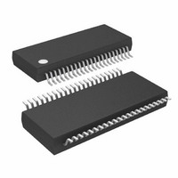
ATMEGA32HVB-8X3 Atmel, ATMEGA32HVB-8X3 Datasheet - Page 67

ATMEGA32HVB-8X3
Manufacturer Part Number
ATMEGA32HVB-8X3
Description
MCU AVR 32KB FLASH 8MHZ 44TSSOP
Manufacturer
Atmel
Series
AVR® ATmegar
Specifications of ATMEGA32HVB-8X3
Core Processor
AVR
Core Size
8-Bit
Speed
8MHz
Connectivity
I²C, SPI
Peripherals
POR, WDT
Number Of I /o
17
Program Memory Size
32KB (16K x 16)
Program Memory Type
FLASH
Eeprom Size
1K x 8
Ram Size
2K x 8
Voltage - Supply (vcc/vdd)
4 V ~ 25 V
Data Converters
A/D 7x12b
Oscillator Type
External
Operating Temperature
-40°C ~ 85°C
Package / Case
44-TSSOP
Processor Series
ATMEGA32x
Core
AVR8
Data Bus Width
8 bit
Data Ram Size
2 KB
Interface Type
SPI, TWI
Maximum Clock Frequency
8 MHz
Number Of Programmable I/os
17
Number Of Timers
2
Maximum Operating Temperature
+ 85 C
Mounting Style
SMD/SMT
Development Tools By Supplier
ATAVRDRAGON, ATSTK500, ATSTK600, ATAVRISP2, ATAVRONEKIT, ATAVRSB200
Minimum Operating Temperature
- 40 C
On-chip Adc
12 bit, 7 Channel
Package
44TSSOP
Device Core
AVR
Family Name
ATmega
Maximum Speed
8 MHz
Operating Supply Voltage
5|9|12|15|18|24 V
For Use With
ATSTK524 - KIT STARTER ATMEGA32M1/MEGA32C1ATSTK600 - DEV KIT FOR AVR/AVR32ATAVRDRAGON - KIT DRAGON 32KB FLASH MEM AVRATSTK500 - PROGRAMMER AVR STARTER KIT
Lead Free Status / RoHS Status
Lead free / RoHS Compliant
Available stocks
Company
Part Number
Manufacturer
Quantity
Price
Company:
Part Number:
ATMEGA32HVB-8X3
Manufacturer:
Atmel
Quantity:
408
- Current page: 67 of 275
- Download datasheet (7Mb)
15. Low Voltage I/O-Ports
15.1
8042B–AVR–06/10
Overview
All low voltage AVR ports have true Read-Modify-Write functionality when used as general digi-
tal I/O ports. This means that the direction of one port pin can be changed without unintentionally
changing the direction of any other pin with the SBI and CBI instructions. The same applies
when changing drive value (if configured as output) or enabling/disabling of pull-up resistors (if
configured as input). All low voltage port pins have individually selectable pull-up resistors with a
supply-voltage invariant resistance. All I/O pins have protection diodes to both V
as indicated in
of parameters.
Figure 15-1. Low Voltage I/O Pin Equivalent Schematic
All registers and bit references in this section are written in general form. A lower case “x” repre-
sents the numbering letter for the port, and a lower case “n” represents the bit number. However,
when using the register or bit defines in a program, the precise form must be used. For example,
PORTB3 for bit no. 3 in Port B, here documented generally as PORTxn. The physical I/O Regis-
ters and bit locations are listed in
Three I/O memory address locations are allocated for each low voltage port, one each for the
Data Register – PORTx, Data Direction Register – DDRx, and the Port Input Pins – PINx. The
Port Input Pins I/O location is read only, while the Data Register and the Data Direction Register
are read/write. However, writing a logic one to a bit in the PINx Register, will result in a toggle in
the corresponding bit in the Data Register. In addition, the Pull-up Disable – PUD bit in MCUCR
disables the pull-up function for all low voltage pins in all ports when set.
Using the I/O port as General Digital I/O is described in
I/O” on page
peripheral features on the device. How each alternate function interferes with the port pin is
described in
full description of the alternate functions.
”Alternate Port Functions” on page
68. Many low voltage port pins are multiplexed with alternate functions for the
Pxn
Figure
15-1. Refer to
”Register Description” on page
C
pin
”Electrical Characteristics” on page 230
72. Refer to the individual module sections for a
ATmega16HVB/32HVB
”Low Voltage Ports as General Digital
"General Digital I/O" for
78.
See Figure
R
Details
pu
Logic
for a complete list
REG
and Ground
67
Related parts for ATMEGA32HVB-8X3
Image
Part Number
Description
Manufacturer
Datasheet
Request
R

Part Number:
Description:
Manufacturer:
Atmel Corporation
Datasheet:

Part Number:
Description:
Manufacturer:
ATMEL Corporation
Datasheet:

Part Number:
Description:
IC AVR MCU 32K 16MHZ 5V 44-QFN
Manufacturer:
Atmel
Datasheet:

Part Number:
Description:
IC AVR MCU 32K 16MHZ 5V 40DIP
Manufacturer:
Atmel
Datasheet:

Part Number:
Description:
IC AVR MCU 32K 16MHZ 5V 44TQFP
Manufacturer:
Atmel
Datasheet:

Part Number:
Description:
IC AVR MCU 32K 16MHZ IND 40-DIP
Manufacturer:
Atmel
Datasheet:

Part Number:
Description:
IC AVR MCU 32K 16MHZ IND 44-TQFP
Manufacturer:
Atmel
Datasheet:

Part Number:
Description:
MCU AVR 32KB FLASH 16MHZ 44TQFP
Manufacturer:
Atmel
Datasheet:

Part Number:
Description:
MCU AVR 32KB FLASH 16MHZ 44QFN
Manufacturer:
Atmel
Datasheet:

Part Number:
Description:
MCU AVR 32K FLASH 16MHZ 44-TQFP
Manufacturer:
Atmel
Datasheet:

Part Number:
Description:
IC AVR MCU 32K 16MHZ COM 40-DIP
Manufacturer:
Atmel
Datasheet:

Part Number:
Description:
IC AVR MCU 32K 16MHZ COM 44-QFN
Manufacturer:
Atmel
Datasheet:

Part Number:
Description:
IC AVR MCU 32K 16MHZ COM 44-TQFP
Manufacturer:
Atmel
Datasheet:


