ATMEGA32HVB-8X3 Atmel, ATMEGA32HVB-8X3 Datasheet - Page 150
ATMEGA32HVB-8X3
Manufacturer Part Number
ATMEGA32HVB-8X3
Description
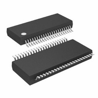
MCU AVR 32KB FLASH 8MHZ 44TSSOP
Manufacturer
Atmel
Series
AVR® ATmegar
Specifications of ATMEGA32HVB-8X3
Core Processor
AVR
Core Size
8-Bit
Speed
8MHz
Connectivity
I²C, SPI
Peripherals
POR, WDT
Number Of I /o
17
Program Memory Size
32KB (16K x 16)
Program Memory Type
FLASH
Eeprom Size
1K x 8
Ram Size
2K x 8
Voltage - Supply (vcc/vdd)
4 V ~ 25 V
Data Converters
A/D 7x12b
Oscillator Type
External
Operating Temperature
-40°C ~ 85°C
Package / Case
44-TSSOP
Processor Series
ATMEGA32x
Core
AVR8
Data Bus Width
8 bit
Data Ram Size
2 KB
Interface Type
SPI, TWI
Maximum Clock Frequency
8 MHz
Number Of Programmable I/os
17
Number Of Timers
2
Maximum Operating Temperature
+ 85 C
Mounting Style
SMD/SMT
Development Tools By Supplier
ATAVRDRAGON, ATSTK500, ATSTK600, ATAVRISP2, ATAVRONEKIT, ATAVRSB200
Minimum Operating Temperature
- 40 C
On-chip Adc
12 bit, 7 Channel
Package
44TSSOP
Device Core
AVR
Family Name
ATmega
Maximum Speed
8 MHz
Operating Supply Voltage
5|9|12|15|18|24 V
For Use With
ATSTK524 - KIT STARTER ATMEGA32M1/MEGA32C1ATSTK600 - DEV KIT FOR AVR/AVR32ATAVRDRAGON - KIT DRAGON 32KB FLASH MEM AVRATSTK500 - PROGRAMMER AVR STARTER KIT
Lead Free Status / RoHS Status
Lead free / RoHS Compliant
Available stocks
Company
Part Number
Manufacturer
Quantity
Price
Company:

Part Number:
ATMEGA32HVB-8X3
Manufacturer:
Atmel
Quantity:
408


25.3.2
8042B–AVR–06/10
DUVR – Deep Under Voltage Recovery Mode without Pre-charge FET
The C-FET/D-FETs is switched on by pumping the gate OC/OD above the source voltage
(PVT/BATT) of the external FET. When the gate-source voltage has reached a level higher than
typically 13V the pumping frequency is reduced and is regulated to maintain the high gate-
source voltage. For low VFET voltages (< 8 Volts) this level is never reached, thus the pumping
frequency is not reduced. The gate-source voltage for low VFET voltages is close to 2VFET-2V.
To avoid over-heating the external FET's when turning them off OC/OD is pulled quickly low.
If the C-FET is disabled and D-FET enabled, discharge current will run through the body-drain
diode of the C-FET and vice versa. To avoid the potential heat problem from this situation, soft-
ware should ensure that the D-FET is not disabled when a large charge current is flowing, and
that the C-FET is not disabled when a large discharge current is flowing.
To allow charging of deeply discharged cells using chargers with pre-charge functionality, the
FET Driver can be configured to operate in Deep Under-Voltage Recovery (DUVR) mode.
DUVR mode allows charging of deeply discharged cells without using an additional pre-charge
FET. To enter Deep Under Voltage Recovery Mode, software should clear the DUVRD bit
(DUVRD=0) in the FET Control and Status Register (FCSR). DUVR mode cannot be used in 2-
cell applications, refer to
In DUVR mode the FET Driver regulates the voltage at VFET quickly to typically 4.5V by partly
opening the C-FET. At this voltage the chip is fully operational. With the C-FET partly open the
charger is allowed to charge the battery with a pre-charge current. As the cell voltage starts to
increase above 4.5V the VFET voltage follows the cell voltage. When the total cell voltage has
been charged to a voltage higher than 5V, it is safe to exit DUVR mode and to turn-on the C-FET
completely. Software should then set the DUVRD bit to exit DUVR and fully open the C-FET by
setting the CFET bit. Note that it is recommended that this is done in two steps.
1. Exit DUVR mode by setting the DUVRD bit.
2. Wait until register synchronization is complete (see guard time notice in
To avoid potential heating of the C-FET and D-FET in DUVR mode, the charger should not be
allowed to enter quick-charge until the FET has been completely enabled and the FET driver
has exit DUVR mode. It is therefore recommended to use the CC-ADC to continuously monitor
the current flowing during DUVR mode charging, and to turn-off the FETs if an illegal charge cur-
rent is measured. For fast tracking, it is recommended to use the CC-ADC Instantaneous
Current Output. For details on CC-ADC usage, see
ing Sigma-delta ADC” on page
Before entering DUVR-mode it is recommended to enable the D-FET. After enabling the D-FET
it is recommended that SW add a hold-off time of 10ms before DUVR mode is entered. This is to
make sure that the D-FET is completely enabled.
To avoid that the charger enters quick-charge before the battery has exit DUVR mode, it is rec-
ommended that either
1. The battery controls when the charger is allowed to enter quick-charge. This is done by
2. The charger itself controls when to enter quick-charge by sensing the voltage at the
Description” on page
communicating to the charger over the SMBus line when the charger is allowed to enter
increase the charge current.
Pack+ terminal. It is not recommended that the charger allows quick-charge until the
charger senses a Pack+ voltage higher than 7V. To avoid potential heating problem SW
”Deep Under Voltage operation with Pre-charge FET” on page
153), and enable the C-FET by setting the CFE bit.
108.
”Coulomb Counter – Dedicated Fuel Gaug-
ATmega16HVB/32HVB
”Register
152.
150
Related parts for ATMEGA32HVB-8X3
Image
Part Number
Description
Manufacturer
Datasheet
Request
R

Part Number:
Description:
Manufacturer:
Atmel Corporation
Datasheet:
Part Number:
Description:
Manufacturer:
ATMEL Corporation
Datasheet:

Part Number:
Description:
IC AVR MCU 32K 16MHZ 5V 44-QFN
Manufacturer:
Atmel
Datasheet:

Part Number:
Description:
IC AVR MCU 32K 16MHZ 5V 40DIP
Manufacturer:
Atmel
Datasheet:

Part Number:
Description:
IC AVR MCU 32K 16MHZ 5V 44TQFP
Manufacturer:
Atmel
Datasheet:
Part Number:
Description:
IC AVR MCU 32K 16MHZ IND 40-DIP
Manufacturer:
Atmel
Datasheet:
Part Number:
Description:
IC AVR MCU 32K 16MHZ IND 44-TQFP
Manufacturer:
Atmel
Datasheet:

Part Number:
Description:
MCU AVR 32KB FLASH 16MHZ 44TQFP
Manufacturer:
Atmel
Datasheet:
Part Number:
Description:
MCU AVR 32KB FLASH 16MHZ 44QFN
Manufacturer:
Atmel
Datasheet:
Part Number:
Description:
MCU AVR 32K FLASH 16MHZ 44-TQFP
Manufacturer:
Atmel
Datasheet:
Part Number:
Description:
IC AVR MCU 32K 16MHZ COM 40-DIP
Manufacturer:
Atmel
Datasheet:
Part Number:
Description:
IC AVR MCU 32K 16MHZ COM 44-QFN
Manufacturer:
Atmel
Datasheet:
Part Number:
Description:
IC AVR MCU 32K 16MHZ COM 44-TQFP
Manufacturer:
Atmel
Datasheet: