ATMEGA32HVB-8X3 Atmel, ATMEGA32HVB-8X3 Datasheet - Page 63
ATMEGA32HVB-8X3
Manufacturer Part Number
ATMEGA32HVB-8X3
Description
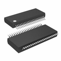
MCU AVR 32KB FLASH 8MHZ 44TSSOP
Manufacturer
Atmel
Series
AVR® ATmegar
Specifications of ATMEGA32HVB-8X3
Core Processor
AVR
Core Size
8-Bit
Speed
8MHz
Connectivity
I²C, SPI
Peripherals
POR, WDT
Number Of I /o
17
Program Memory Size
32KB (16K x 16)
Program Memory Type
FLASH
Eeprom Size
1K x 8
Ram Size
2K x 8
Voltage - Supply (vcc/vdd)
4 V ~ 25 V
Data Converters
A/D 7x12b
Oscillator Type
External
Operating Temperature
-40°C ~ 85°C
Package / Case
44-TSSOP
Processor Series
ATMEGA32x
Core
AVR8
Data Bus Width
8 bit
Data Ram Size
2 KB
Interface Type
SPI, TWI
Maximum Clock Frequency
8 MHz
Number Of Programmable I/os
17
Number Of Timers
2
Maximum Operating Temperature
+ 85 C
Mounting Style
SMD/SMT
Development Tools By Supplier
ATAVRDRAGON, ATSTK500, ATSTK600, ATAVRISP2, ATAVRONEKIT, ATAVRSB200
Minimum Operating Temperature
- 40 C
On-chip Adc
12 bit, 7 Channel
Package
44TSSOP
Device Core
AVR
Family Name
ATmega
Maximum Speed
8 MHz
Operating Supply Voltage
5|9|12|15|18|24 V
For Use With
ATSTK524 - KIT STARTER ATMEGA32M1/MEGA32C1ATSTK600 - DEV KIT FOR AVR/AVR32ATAVRDRAGON - KIT DRAGON 32KB FLASH MEM AVRATSTK500 - PROGRAMMER AVR STARTER KIT
Lead Free Status / RoHS Status
Lead free / RoHS Compliant
Available stocks
Company
Part Number
Manufacturer
Quantity
Price
Company:

Part Number:
ATMEGA32HVB-8X3
Manufacturer:
Atmel
Quantity:
408


14.2
14.2.1
14.2.2
8042B–AVR–06/10
High Voltage Ports as General Digital I/O
Configuring the Pin
Reading the Pin
The high voltage ports are high voltage tolerant open collector output ports. In addition they can
be used as general digital inputs.
pin, here generically called Pxn.
Figure 14-2. General High Voltage Digital I/O
Notes:
Each port pin consist of two register bits: PORTxn and PINxn. As shown in
tion” on page
the PINx I/O address.
If PORTxn is written logic one, the port pin is driven low (zero). If PORTxn is written logic zero,
the port pin is tri-stated. The port pins are tri-stated when a reset condition becomes active, even
if no clocks are running.
The port pin can be read through the PINxn Register bit. As shown in
Register bit and the preceding latch constitute a synchronizer. This is needed to avoid metasta-
bility if the physical pin changes value near the edge of the internal clock, but it also introduces a
delay.
1. WRx, RRx and RPx are common to all pins within the same port. clk
2. The High Voltage Digital Input is not present on PC5.
mon to all ports.
Pxn
66, the PORTxn bits are accesed at the PORTx I/O address, and the PINxn bits at
SLEEP:
clkI/O:
HIGH VOLTAGE DIGITAL INPUT
SLEEP CONTROL
I/O CLOCK
Figure 14-2
SLEEP
(2)
shows a functional description of one output port
(1)
SYNCHRONIZER
RRx:
WRx:
RPx:
ATmega16HVB/32HVB
D
L
RESET
CLR
SET
PORTxn
Q
Q
_
CLR
Q
_
Q
READ PORTx REGISTER
WRITE PORTx REGISTER
READ PINx REGISTER
D
D
PINxn
CLR
Q
_
Q
RRx
WRx
clk
RPx
Figure
I/O
I/O
and SLEEP are com-
”Register Descrip-
14-2, the PINxn
63
Related parts for ATMEGA32HVB-8X3
Image
Part Number
Description
Manufacturer
Datasheet
Request
R

Part Number:
Description:
Manufacturer:
Atmel Corporation
Datasheet:
Part Number:
Description:
Manufacturer:
ATMEL Corporation
Datasheet:

Part Number:
Description:
IC AVR MCU 32K 16MHZ 5V 44-QFN
Manufacturer:
Atmel
Datasheet:

Part Number:
Description:
IC AVR MCU 32K 16MHZ 5V 40DIP
Manufacturer:
Atmel
Datasheet:

Part Number:
Description:
IC AVR MCU 32K 16MHZ 5V 44TQFP
Manufacturer:
Atmel
Datasheet:
Part Number:
Description:
IC AVR MCU 32K 16MHZ IND 40-DIP
Manufacturer:
Atmel
Datasheet:
Part Number:
Description:
IC AVR MCU 32K 16MHZ IND 44-TQFP
Manufacturer:
Atmel
Datasheet:

Part Number:
Description:
MCU AVR 32KB FLASH 16MHZ 44TQFP
Manufacturer:
Atmel
Datasheet:
Part Number:
Description:
MCU AVR 32KB FLASH 16MHZ 44QFN
Manufacturer:
Atmel
Datasheet:
Part Number:
Description:
MCU AVR 32K FLASH 16MHZ 44-TQFP
Manufacturer:
Atmel
Datasheet:
Part Number:
Description:
IC AVR MCU 32K 16MHZ COM 40-DIP
Manufacturer:
Atmel
Datasheet:
Part Number:
Description:
IC AVR MCU 32K 16MHZ COM 44-QFN
Manufacturer:
Atmel
Datasheet:
Part Number:
Description:
IC AVR MCU 32K 16MHZ COM 44-TQFP
Manufacturer:
Atmel
Datasheet: