ATMEGA32HVB-8X3 Atmel, ATMEGA32HVB-8X3 Datasheet - Page 38
ATMEGA32HVB-8X3
Manufacturer Part Number
ATMEGA32HVB-8X3
Description
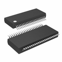
MCU AVR 32KB FLASH 8MHZ 44TSSOP
Manufacturer
Atmel
Series
AVR® ATmegar
Specifications of ATMEGA32HVB-8X3
Core Processor
AVR
Core Size
8-Bit
Speed
8MHz
Connectivity
I²C, SPI
Peripherals
POR, WDT
Number Of I /o
17
Program Memory Size
32KB (16K x 16)
Program Memory Type
FLASH
Eeprom Size
1K x 8
Ram Size
2K x 8
Voltage - Supply (vcc/vdd)
4 V ~ 25 V
Data Converters
A/D 7x12b
Oscillator Type
External
Operating Temperature
-40°C ~ 85°C
Package / Case
44-TSSOP
Processor Series
ATMEGA32x
Core
AVR8
Data Bus Width
8 bit
Data Ram Size
2 KB
Interface Type
SPI, TWI
Maximum Clock Frequency
8 MHz
Number Of Programmable I/os
17
Number Of Timers
2
Maximum Operating Temperature
+ 85 C
Mounting Style
SMD/SMT
Development Tools By Supplier
ATAVRDRAGON, ATSTK500, ATSTK600, ATAVRISP2, ATAVRONEKIT, ATAVRSB200
Minimum Operating Temperature
- 40 C
On-chip Adc
12 bit, 7 Channel
Package
44TSSOP
Device Core
AVR
Family Name
ATmega
Maximum Speed
8 MHz
Operating Supply Voltage
5|9|12|15|18|24 V
For Use With
ATSTK524 - KIT STARTER ATMEGA32M1/MEGA32C1ATSTK600 - DEV KIT FOR AVR/AVR32ATAVRDRAGON - KIT DRAGON 32KB FLASH MEM AVRATSTK500 - PROGRAMMER AVR STARTER KIT
Lead Free Status / RoHS Status
Lead free / RoHS Compliant
Available stocks
Company
Part Number
Manufacturer
Quantity
Price
Company:

Part Number:
ATMEGA32HVB-8X3
Manufacturer:
Atmel
Quantity:
408


10.5
10.6
10.7
10.7.1
10.7.2
8042B–AVR–06/10
Power-off Mode
Power Reduction Register
Minimizing Power Consumption
Watchdog Timer
Port Pins
If the current through the sense resistor is so small that the Coulomb Counter cannot measure it
accurately, Regular Current detection should be enabled to reduce power consumption. The
WDT keeps accurately track of the time so that battery self discharge can be calculated.
Note that if a level triggered interrupt is used for wake-up from Power-save mode, the changed
level must be held for some time to wake up the MCU. Refer to
for details.
When waking up from Power-save mode, there is a delay from the wake-up condition occurs
until the wake-up becomes effective. This allows the clock to restart and become stable after
having been stopped. The wake-up period is defined in
When the SM2..0 bits are written to 100 and the SE bit is set, the SLEEP instruction makes the
CPU shut down the Voltage Regulator, leaving only the Charger Detect Circuitry operational. To
ensure that the MCU enters Power-off mode only when intended, the SLEEP instruction must be
executed within 4 clock cycles after the SM2..0 bits are written. The MCU will reset when return-
ing from Power-off mode.
Note:
The Power Reduction Register (PRR), see
provides a method to stop the clock to individual peripherals to reduce power consumption. The
current state of the peripheral is frozen and the I/O registers can not be read or written.
Resources used by the peripheral when stopping the clock will remain occupied, hence the
peripheral should in most cases be disabled before stopping the clock. Waking up a module,
which is done by clearing the bit in PRR, puts the module in the same state as before shutdown.
Module shutdown can be used in Idle mode and Active mode to significantly reduce the overall
power consumption. In all other sleep modes, the clock is already stopped.
There are several issues to consider when trying to minimize the power consumption in an AVR
controlled system. In general, sleep modes should be used as much as possible, and the sleep
mode should be selected so that as few as possible of the device’s functions are operating. All
functions not needed should be disabled. In particular, the following modules may need special
consideration when trying to achieve the lowest possible power consumption.
If the Watchdog Timer is not needed in the application, the module should be turned off. If the
Watchdog Timer is enabled, it will be enabled in all sleep modes except Power-off. The Watch-
dog Timer current consumption is significant only in Power-save mode. Refer to
Timer” on page 46
When entering a sleep mode, all port pins should be configured to use minimum power. The
most important is then to ensure that no pins drive resistive loads. In sleep modes where both
the I/O clock (clk
be disabled. This ensures that no power is consumed by the input logic when not needed. In
Before entering Power-off sleep mode, interrupts should be disabled by software. Otherwise inter-
rupts may prevent the SLEEP instruction from being executed within the time limit.
I/O
for details on how to configure the Watchdog Timer.
) and the ADC clock (clk
ADC
”PRR0 – Power Reduction Register 0” on page
) are stopped, the input buffers of the device will
ATmega16HVB/32HVB
”Clock Sources” on page
”External Interrupts” on page 58
26.
”Watchdog
40,
38
Related parts for ATMEGA32HVB-8X3
Image
Part Number
Description
Manufacturer
Datasheet
Request
R

Part Number:
Description:
Manufacturer:
Atmel Corporation
Datasheet:
Part Number:
Description:
Manufacturer:
ATMEL Corporation
Datasheet:

Part Number:
Description:
IC AVR MCU 32K 16MHZ 5V 44-QFN
Manufacturer:
Atmel
Datasheet:

Part Number:
Description:
IC AVR MCU 32K 16MHZ 5V 40DIP
Manufacturer:
Atmel
Datasheet:

Part Number:
Description:
IC AVR MCU 32K 16MHZ 5V 44TQFP
Manufacturer:
Atmel
Datasheet:
Part Number:
Description:
IC AVR MCU 32K 16MHZ IND 40-DIP
Manufacturer:
Atmel
Datasheet:
Part Number:
Description:
IC AVR MCU 32K 16MHZ IND 44-TQFP
Manufacturer:
Atmel
Datasheet:

Part Number:
Description:
MCU AVR 32KB FLASH 16MHZ 44TQFP
Manufacturer:
Atmel
Datasheet:
Part Number:
Description:
MCU AVR 32KB FLASH 16MHZ 44QFN
Manufacturer:
Atmel
Datasheet:
Part Number:
Description:
MCU AVR 32K FLASH 16MHZ 44-TQFP
Manufacturer:
Atmel
Datasheet:
Part Number:
Description:
IC AVR MCU 32K 16MHZ COM 40-DIP
Manufacturer:
Atmel
Datasheet:
Part Number:
Description:
IC AVR MCU 32K 16MHZ COM 44-QFN
Manufacturer:
Atmel
Datasheet:
Part Number:
Description:
IC AVR MCU 32K 16MHZ COM 44-TQFP
Manufacturer:
Atmel
Datasheet: