ATMEGA32HVB-8X3 Atmel, ATMEGA32HVB-8X3 Datasheet - Page 153
ATMEGA32HVB-8X3
Manufacturer Part Number
ATMEGA32HVB-8X3
Description
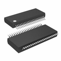
MCU AVR 32KB FLASH 8MHZ 44TSSOP
Manufacturer
Atmel
Series
AVR® ATmegar
Specifications of ATMEGA32HVB-8X3
Core Processor
AVR
Core Size
8-Bit
Speed
8MHz
Connectivity
I²C, SPI
Peripherals
POR, WDT
Number Of I /o
17
Program Memory Size
32KB (16K x 16)
Program Memory Type
FLASH
Eeprom Size
1K x 8
Ram Size
2K x 8
Voltage - Supply (vcc/vdd)
4 V ~ 25 V
Data Converters
A/D 7x12b
Oscillator Type
External
Operating Temperature
-40°C ~ 85°C
Package / Case
44-TSSOP
Processor Series
ATMEGA32x
Core
AVR8
Data Bus Width
8 bit
Data Ram Size
2 KB
Interface Type
SPI, TWI
Maximum Clock Frequency
8 MHz
Number Of Programmable I/os
17
Number Of Timers
2
Maximum Operating Temperature
+ 85 C
Mounting Style
SMD/SMT
Development Tools By Supplier
ATAVRDRAGON, ATSTK500, ATSTK600, ATAVRISP2, ATAVRONEKIT, ATAVRSB200
Minimum Operating Temperature
- 40 C
On-chip Adc
12 bit, 7 Channel
Package
44TSSOP
Device Core
AVR
Family Name
ATmega
Maximum Speed
8 MHz
Operating Supply Voltage
5|9|12|15|18|24 V
For Use With
ATSTK524 - KIT STARTER ATMEGA32M1/MEGA32C1ATSTK600 - DEV KIT FOR AVR/AVR32ATAVRDRAGON - KIT DRAGON 32KB FLASH MEM AVRATSTK500 - PROGRAMMER AVR STARTER KIT
Lead Free Status / RoHS Status
Lead free / RoHS Compliant
Available stocks
Company
Part Number
Manufacturer
Quantity
Price
Company:

Part Number:
ATMEGA32HVB-8X3
Manufacturer:
Atmel
Quantity:
408


25.4
25.4.1
8042B–AVR–06/10
Register Description
FCSR – FET Control and Status Register
• Bits 7:4 – Reserved
These bits are reserved in the ATmega16HVB/32HVB, and will always read as zero.
• Bit 3 – DUVRD: Deep Under-voltage Recovery Disabled
When the DUVRD is cleared (zero), the FET Driver will be forced to operate in Deep Under-volt-
age Recovery DUVR mode. See
charge FET” on page 150
during current protection or during internal reset, the DUVRD bit is overridden to one by hard-
ware in these cases. When this bit is set (one), Deep Under-voltage Recovery mode of the FET
Driver will be disabled. DUVR mode should not be used in 2-cell applications.
• Bit 2 – CPS: Current Protection Status
The CPS bit shows the status of the Current Protection. This bit is set (one) when a Current Pro-
tection is active, and cleared (zero) otherwise.
• Bit 1 – DFE: Discharge FET Enable
When the DFE bit is cleared (zero), the Discharge FET will be disabled regardless of the state of
the Battery Protection circuitry. When this bit is set (one), the Discharge FET is enabled. This bit
will automatically be cleared by the CBP circuitry when Current Protection is activated. When
this bit is cleared, Short-circuit, Discharge High-current and Discharge Over-current are disabled
regardless of the settings in the BPCR Register.
• Bit 0 – CFE: Charge FET Enable
When the CFE bit is cleared (zero), the Charge FET will be disabled regardless of the state of
the Battery Protection circuitry. When this bit is set (one), the Charge FET is enabled. This bit
will automatically be cleared by the CBP circuitry when Current Protection is activated. When
this bit is cleared and the DUVRD bit is set, Charge High-current Protection and Charge Over-
current Protection are disabled regardless of the settings in the BPCR Register. When the
DUVRD bit is cleared, the charge FET will be enabled by DUVR mode regardless of the CFE
status.
Notes:
Bit
(0xF0)
Read/Write
Initial Value
1. Due to synchronization of parameters between clock domains, a guard time of 3 ULP oscillator
2. The NFET drivers require a minimum total cell voltage of 6V or higher or a charger connected
cycles + 3 CPU clock cycles is required between each time the FCSR register is written. Any
writing to the FCSR register during this period will be ignored.
to turn-on the FETs. Note that this limit only applies if the FET is disabled in advanced. If the
FET is already enabled, the FET will be fully operational in the entire voltage range of the
device (4-25V).
R
7
–
0
R
6
–
0
for details. To avoid that the FET driver tries to switch on the C-FET
R
”DUVR – Deep Under Voltage Recovery Mode without Pre-
5
–
0
R
4
–
0
DUVRD
ATmega16HVB/32HVB
R/W
3
1
CPS
R
2
0
DFE
R/W
1
0
CFE
R/W
0
0
FCSR
153
Related parts for ATMEGA32HVB-8X3
Image
Part Number
Description
Manufacturer
Datasheet
Request
R

Part Number:
Description:
Manufacturer:
Atmel Corporation
Datasheet:
Part Number:
Description:
Manufacturer:
ATMEL Corporation
Datasheet:

Part Number:
Description:
IC AVR MCU 32K 16MHZ 5V 44-QFN
Manufacturer:
Atmel
Datasheet:

Part Number:
Description:
IC AVR MCU 32K 16MHZ 5V 40DIP
Manufacturer:
Atmel
Datasheet:

Part Number:
Description:
IC AVR MCU 32K 16MHZ 5V 44TQFP
Manufacturer:
Atmel
Datasheet:
Part Number:
Description:
IC AVR MCU 32K 16MHZ IND 40-DIP
Manufacturer:
Atmel
Datasheet:
Part Number:
Description:
IC AVR MCU 32K 16MHZ IND 44-TQFP
Manufacturer:
Atmel
Datasheet:

Part Number:
Description:
MCU AVR 32KB FLASH 16MHZ 44TQFP
Manufacturer:
Atmel
Datasheet:
Part Number:
Description:
MCU AVR 32KB FLASH 16MHZ 44QFN
Manufacturer:
Atmel
Datasheet:
Part Number:
Description:
MCU AVR 32K FLASH 16MHZ 44-TQFP
Manufacturer:
Atmel
Datasheet:
Part Number:
Description:
IC AVR MCU 32K 16MHZ COM 40-DIP
Manufacturer:
Atmel
Datasheet:
Part Number:
Description:
IC AVR MCU 32K 16MHZ COM 44-QFN
Manufacturer:
Atmel
Datasheet:
Part Number:
Description:
IC AVR MCU 32K 16MHZ COM 44-TQFP
Manufacturer:
Atmel
Datasheet: