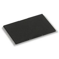
H27UAG8T2ATR-BC HYNIX SEMICONDUCTOR, H27UAG8T2ATR-BC Datasheet - Page 56

H27UAG8T2ATR-BC
Manufacturer Part Number
H27UAG8T2ATR-BC
Description
58T1891
Manufacturer
HYNIX SEMICONDUCTOR
Datasheet
1.H27UAG8T2ATR-BC.pdf
(61 pages)
Specifications of H27UAG8T2ATR-BC
Memory Type
Flash - NAND
Memory Size
16Gbit
Memory Configuration
2048M X 8
Supply Voltage Range
2.7V To 3.6V
Memory Case Style
TSOP
No. Of Pins
48
Operating Temperature Range
0°C To +70°C
Rohs Compliant
Yes
Available stocks
Company
Part Number
Manufacturer
Quantity
Price
Company:
Part Number:
H27UAG8T2ATR-BC
Manufacturer:
HYNIX
Quantity:
2 526
Company:
Part Number:
H27UAG8T2ATR-BC
Manufacturer:
SIEMENS
Quantity:
390
Company:
Part Number:
H27UAG8T2ATR-BC
Manufacturer:
HYNIX
Quantity:
4 000
Part Number:
H27UAG8T2ATR-BC
Manufacturer:
HYNIX/海力士
Quantity:
20 000
Rev 1.0 / Aug. 2010
6. OTHER FEATURES
6.1. Data Protection & Power on/off Sequence
The device is designed to offer protection from any involuntary program/erase during power-transitions. An internal
voltage detector disables all functions whenever V
protection and is recommended to be kept at VIL during power-up and power-down.
The reset command (FFh) must be issued to all dies as the first command after device is power up. Each R/B# will be
busy for maximum of 2ms after reset command is issued. In this time, the acceptable command is 70h or 78h.
6.2. Ready / Busy
The device has a Ready/Busy output that provides method of indicating the completion of a page program, erase,
copy-back and random read completion. The R/B# pin is normally high and goes to low when the device is busy (after
a reset, read, program, and erase operation). It returns to high when the internal controller has finished the operation.
The pin is an open-drain driver thereby allowing two or more R/B# outputs to be Or-tied. Because pull-up resistor
value is related to tR (R/B#) and current drain during busy (Ibusy), an appropriate value can be obtained with the fol-
lowing reference chart (Figure 58). Its value can be determined by the following guidance.
■ Figure 57. Data protection and power on / off
WP#
CLE
WE#
ALE
RE#
I/Ox
R/B#
VCC
CE#
0V
Vcc ramp
starts
3V device = 2.7V
(min)
(max)
50
10
1
ms
(max)
CC
is below about 2.0V (3.3V device). WP# pin provides hardware
t CS
FFh
16Gb (2048M x 8bit) NAND Flash
(max)
2
ms
: Don’t care
H27UAG8T2B Series
: Undefined
2.7V
Release
56


