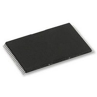
H27UAG8T2ATR-BC HYNIX SEMICONDUCTOR, H27UAG8T2ATR-BC Datasheet - Page 45

H27UAG8T2ATR-BC
Manufacturer Part Number
H27UAG8T2ATR-BC
Description
58T1891
Manufacturer
HYNIX SEMICONDUCTOR
Datasheet
1.H27UAG8T2ATR-BC.pdf
(61 pages)
Specifications of H27UAG8T2ATR-BC
Memory Type
Flash - NAND
Memory Size
16Gbit
Memory Configuration
2048M X 8
Supply Voltage Range
2.7V To 3.6V
Memory Case Style
TSOP
No. Of Pins
48
Operating Temperature Range
0°C To +70°C
Rohs Compliant
Yes
Available stocks
Company
Part Number
Manufacturer
Quantity
Price
Company:
Part Number:
H27UAG8T2ATR-BC
Manufacturer:
HYNIX
Quantity:
2 526
Company:
Part Number:
H27UAG8T2ATR-BC
Manufacturer:
SIEMENS
Quantity:
390
Company:
Part Number:
H27UAG8T2ATR-BC
Manufacturer:
HYNIX
Quantity:
4 000
Part Number:
H27UAG8T2ATR-BC
Manufacturer:
HYNIX/海力士
Quantity:
20 000
Rev 1.0 / Aug. 2010
tus bit (I/O 6). In addition, the status bit (I/O 5) can be used to determine when the cell programming of the current
data register contents is complete. Pass/fail status of only the previous page (I/O 1) is available upon the return to
Ready state.
The last page of the target programming sequence must be programmed with actual “Page Program” command (10h).
If single plane cache program begins, single plane sequence should be used until single plane cache program is ended.
Pass/fail status is available in two steps. I/O 1 returns with the status of the previous page upon Ready or I/O6 status
bit changing to "1", and later I/O 0 with the status of current page upon true Ready (returning from internal program-
ming) or I/O 5 status bit changing to "1". I/O 1 may be read together when I/O 0 is checked. Refer to 2.8. Status
Register Coding and Figure 43 for more details.
■ Figure 43. Cache program
R/B#
R/B#
R/B#
I/Ox
I/Ox
I/Ox
R/B# Pin
Data Cache Ready /Bysy
(I/O6)
Data Cache Ready /Bysy
(I/O5)
Pass / Fail status for each page programmed by the Cache Program operation can be detected by the Read Status operation.
The Pass / Fail status on I/O 0 and I/O 1 are valid under the following conditions.
The Ready/ Busy is output on I/O 5 by Read Status operation or R/B pin after the 10h command.
The Data Cache Ready / Busy is output on I/O 6 by Read Status operation or R/B pin after the 15h command.
I/O 0 : Pass / Fail of the current page program operation.
I/O 1 : Pass / Fail of the previous page program operation.
Status on I/O 0 : Ready / Busy is Ready state.
Status on I/O 1 : Data Cache Ready / Busy is Ready State.
80h-add-data-15h
A
B
Page 1
I/O 1 =>
I/O 0 =>
80h
80h
80h
t
CBSYW
70h
Address (5 cycle)
Address (5 cycle)
Invalid
Invalid
Address (5 cycle)
OUT
SR
Page 1
80h-add-data-15h
Page 2
t
CBSYW
70h
Page 2
Page1
Invalid
Data Input
OUT
Data Input
SR
Data Input
70h
During both I/O6 and I/O5 return to high, the Pass/Fail for previous page and current page
can be shown through I/O1 and I/O0 concurrently.
Page1
Page2
OUT
SR
80h-add-data-15h
15h
15h
10h
Page N-1
16Gb (2048M x 8bit) NAND Flash
t
CBSYW
t
70h
t
CBSYW
CBSYW
Page N-2
Invalid
OUT
SR
t
PROG
Page N-1
80h-add-data-15h
H27UAG8T2B Series
Page N
A
B
70h
70h
t
PROG
Invalid
Invalid
Page N
OUT
SR
Release
Status
70h
Page N-1
Page N
OUT
SR
45


