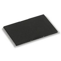
H27UAG8T2ATR-BC HYNIX SEMICONDUCTOR, H27UAG8T2ATR-BC Datasheet - Page 39

H27UAG8T2ATR-BC
Manufacturer Part Number
H27UAG8T2ATR-BC
Description
58T1891
Manufacturer
HYNIX SEMICONDUCTOR
Datasheet
1.H27UAG8T2ATR-BC.pdf
(61 pages)
Specifications of H27UAG8T2ATR-BC
Memory Type
Flash - NAND
Memory Size
16Gbit
Memory Configuration
2048M X 8
Supply Voltage Range
2.7V To 3.6V
Memory Case Style
TSOP
No. Of Pins
48
Operating Temperature Range
0°C To +70°C
Rohs Compliant
Yes
Available stocks
Company
Part Number
Manufacturer
Quantity
Price
Company:
Part Number:
H27UAG8T2ATR-BC
Manufacturer:
HYNIX
Quantity:
2 526
Company:
Part Number:
H27UAG8T2ATR-BC
Manufacturer:
SIEMENS
Quantity:
390
Company:
Part Number:
H27UAG8T2ATR-BC
Manufacturer:
HYNIX
Quantity:
4 000
Part Number:
H27UAG8T2ATR-BC
Manufacturer:
HYNIX/海力士
Quantity:
20 000
Rev 1.0 / Aug. 2010
4.2. Cache Read (available only within a block)
To improve page read throughput, cache read operation is used within a block. First step is same as normal page read,
issuing a page read sequence (00-30h). After random access (R/B# returns to high), 31h command is latched into the
command register. Data is being transferred from the data register to the cache register. While cache register data is
outputted, next page is transferred from memory cell to data register. R/B# will stay low during present page random
accessing and previous page transferring to cache register. Because it is not necessary to output a whole page data
before issuing another 31h command, if serial data output time exceeds random access time (t
time can be hidden. The subsequent pages are issued additional 31h commands. To terminate cache read, 3Fh com-
mand should be issued. This command transfer data from data register to the cache register without issuing next page
read. During the Cache Read Operation, device doesn't allow any other command except Cache Read command (31h),
Read Status (70h, 78h), Read (00h), and Reset (FFh). To carry out other operations after cache operation, cache read
must be ended by 3Fh command or issue reset (FFh) before next operation.
4.3. Multi Plane Page Read
Multi plane Page Read is an extension of Page Read, for a single plane with 8640byte page registers. Since the device
is equipped with two memory planes, activating the two sets of 8640byte page resisters enables a random read of two
pages. Multi plane Page Read is initiated by repeating command 60h followed by three address cycles twice. In this
case, only same page can be selected from each plane.
After Read Confirm command (30h) the 17280bytes of data within the selected two pages are transferred to the data
registers in less than 200㎲ (t
the output of R/B# pin.
Once the data is loaded into the data registers, the data output of first plane can be read out by issuing command 00h
with Five Address Cycles, command 05h with two column address and finally E0h. The data output of second plane
can be read out using the identical command sequences. The restrictions for multi plane Page Read are shown in Fig-
ure 35. multi plane Page Read must be used in the block which has been programmed with Multi plane Page Program.
■ Figure 34. Cache read
R/B#
WE#
CLE
RE#
I/Ox
As defined for Read
30h
t
R
31h
R
). The system controller can detect the completion of data transfer (t
t
CBSYR
Column 0
D0
...
Dn
31h
t
CBSYR
16Gb (2048M x 8bit) NAND Flash
Column 0
D0
...
Dn
3Fh
H27UAG8T2B Series
t
CBSYR
R
), the random access
Column 0
D0
R
) by monitoring
...
Release
Dn
39


