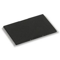
H27UAG8T2ATR-BC HYNIX SEMICONDUCTOR, H27UAG8T2ATR-BC Datasheet - Page 44

H27UAG8T2ATR-BC
Manufacturer Part Number
H27UAG8T2ATR-BC
Description
58T1891
Manufacturer
HYNIX SEMICONDUCTOR
Datasheet
1.H27UAG8T2ATR-BC.pdf
(61 pages)
Specifications of H27UAG8T2ATR-BC
Memory Type
Flash - NAND
Memory Size
16Gbit
Memory Configuration
2048M X 8
Supply Voltage Range
2.7V To 3.6V
Memory Case Style
TSOP
No. Of Pins
48
Operating Temperature Range
0°C To +70°C
Rohs Compliant
Yes
Available stocks
Company
Part Number
Manufacturer
Quantity
Price
Company:
Part Number:
H27UAG8T2ATR-BC
Manufacturer:
HYNIX
Quantity:
2 526
Company:
Part Number:
H27UAG8T2ATR-BC
Manufacturer:
SIEMENS
Quantity:
390
Company:
Part Number:
H27UAG8T2ATR-BC
Manufacturer:
HYNIX
Quantity:
4 000
Part Number:
H27UAG8T2ATR-BC
Manufacturer:
HYNIX/海力士
Quantity:
20 000
Rev 1.0 / Aug. 2010
4.8. Multi Plane Program
Device supports multiple plane program. It is possible to program in parallel 2 pages, one per each plane.
A multiple plane program cycle consists of a double serial data loading period in which up to 17,280bytes of data may
be loaded into the data register, followed by a non-volatile programming period where the loaded data is programmed
into the appropriate cell. The serial data loading period begins by inputting the Serial Data Input command (80h), fol-
lowed by the five cycle address inputs and then serial data for the 1st page. Address for this page must be within first
plane (A<22>=0). The data of first page other than those to be programmed do not need to be loaded. The device
supports random data input exactly like page program operation. The Dummy Page Program Confirm command (11h)
stops 1st page data input and the device becomes busy for a short time (t
command must be issued, followed by second page address (5 cycles) and its serial data input. Address for this page
must be within second plane (A<22>=1). The data of second page other than those to be programmed do not need
to be loaded. Program Confirm command (10h) makes parallel programming of both pages start. User can check oper-
ation status by R/B# pin or read status register command, as if it were a normal page program; status register com-
mand is also available during Dummy Busy time (t
bit of status register will be set: Pass/Fail status of each plane can be checked by Multi Plane Read Status. Figure 42
details the sequence.
Notes:
4.9. Cache Program (available only within a block)
Cache Program is an extension of the standard page program, which is executed with 8,640 bytes cache registers and
same bytes data register. After the serial data input command (80h) is loaded to the command register, followed by 5
cycles of address, a full or partial page of data is latched into the cache register, and then the cache write command
(15h) is loaded to the command register. After that sequence, the data in the cache register is transferred into the data
register for cell programming. At this time, the device remains in busy state. After all data of the cache register is
transferred into the data register, the device goes to the Ready state to load the next data into the cache register by
issuing another cache program command sequence (80h-15h).
There are some restrictions for cache program operation.
1. The cache program command is available only within a block.
2. User must give address and data after 80h command.
The Busy time of first sequence equals the time it takes to transfer the data of cache register to the data register. Cell
programming of the data of data register and loading of the next data into the cache register is consequently pro-
cessed as a pipeline method. On the second and cascading sequence, transfer from the cache register to the data reg-
ister is held off until cell programming of current data register contents has been done.
Read Status command (70h) may be issued to find out when the cache register is ready by polling the Cache-Busy sta-
■
1.
2.
3.
4.
5.
Figure 42. Multi plane page program
R/B#
R/B#
I/Ox
I/Ox
Selected Page address except for A22 within two blocks must be same.
Plane 0 and Plane 1 should be selected within the same chip
Only one block should be selected from the each Plane.
Any command between 11h and 81h is prohibited except 70h/78h and FFh.
Read Status command can be 70h or 78h.
A
80h
81h
2
Address (5 cycle)
1
Address (5 cycle)
nd
st
plane address
plane address
DBSY
Data Input
Data Input
). In case of fail in first plane or second plane page program, fail
10h
11h
16Gb (2048M x 8bit) NAND Flash
DBSY
). Once it has become ready again, 81h
t
DBSY
t
PROG
H27UAG8T2B Series
A
70h
Release
Status
44


