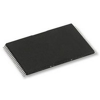
H27UAG8T2ATR-BC HYNIX SEMICONDUCTOR, H27UAG8T2ATR-BC Datasheet - Page 43

H27UAG8T2ATR-BC
Manufacturer Part Number
H27UAG8T2ATR-BC
Description
58T1891
Manufacturer
HYNIX SEMICONDUCTOR
Datasheet
1.H27UAG8T2ATR-BC.pdf
(61 pages)
Specifications of H27UAG8T2ATR-BC
Memory Type
Flash - NAND
Memory Size
16Gbit
Memory Configuration
2048M X 8
Supply Voltage Range
2.7V To 3.6V
Memory Case Style
TSOP
No. Of Pins
48
Operating Temperature Range
0°C To +70°C
Rohs Compliant
Yes
Available stocks
Company
Part Number
Manufacturer
Quantity
Price
Company:
Part Number:
H27UAG8T2ATR-BC
Manufacturer:
HYNIX
Quantity:
2 526
Company:
Part Number:
H27UAG8T2ATR-BC
Manufacturer:
SIEMENS
Quantity:
390
Company:
Part Number:
H27UAG8T2ATR-BC
Manufacturer:
HYNIX
Quantity:
4 000
Part Number:
H27UAG8T2ATR-BC
Manufacturer:
HYNIX/海力士
Quantity:
20 000
Rev 1.0 / Aug. 2010
4.7. Page Program
The device is programmed as a page unit. The number of consecutive partial page programming operation within the
same page without an intervening erase operation must not exceed 1 times. The program addressing should be done
in sequential order in a block. A page program cycle consists of a serial data loading period in which up to 8640bytes
of data may be loaded into the data register, followed by a non-volatile programming period where the loaded data is
programmed into the appropriate cell. The serial data-loading period begins by inputting the Serial Data Input com-
mand (80h), followed by the five cycle address inputs and then serial data. The bytes other than those to be pro-
grammed do not need to be loaded. The device supports random data input in a page. The column address of next
data, which will be entered, may be changed to the address which follows random data input command (85h). Ran-
dom data input may be operated multiple times, regardless of how many times it is done in a page. The Page Program
Confirm command (10h) initiates the programming process. Writing 10h alone without previously entering the serial
data will not initiate the programming process. The internal write state controller automatically executes the algo-
rithms and timings necessary for program and verify, thereby freeing the system controller for other tasks. Once the
program process starts, the Read Status Register command may be entered to read the status register.
The system controller can detect the completion of a program cycle by monitoring the R/B# output, or the Status bit
(I/O 6) of the Status Register. Only the Read Status command and Reset command are valid while programming is in
progress. The Write Status Bit (I/O 0) is valid, when all internal operations are complete (status bit I/O 6 = high).
The internal write verify detects only errors for "1"s that are not successfully programmed to "0"s.
The command register remains in Read Status command mode until another valid command is written to the com-
mand register. Figure 40 and Figure 41 details the sequence.
■
■
Figure 40. Page Program
Figure 41. Random data input
RE#
CLE
CE#
WE#
I/Ox
ALE
R/B#
R/B#
I/Ox
80h
80h
Address
(5 Cycle)
Address 5 cycle
Data
Input
85h
Column address
Address
(2 Cycle)
Data Input
Input
Data
16Gb (2048M x 8bit) NAND Flash
10h
10h
t
PROG
H27UAG8T2B Series
t
PROG
70h
I/O 0 = 0 PROGRAM Pass
I/O 0 = 1 PROGRAM Fail
70h
Status
Release
Status
43


