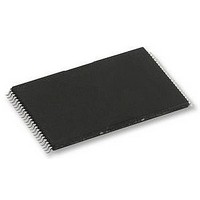
H27UAG8T2ATR-BC HYNIX SEMICONDUCTOR, H27UAG8T2ATR-BC Datasheet - Page 41

H27UAG8T2ATR-BC
Manufacturer Part Number
H27UAG8T2ATR-BC
Description
58T1891
Manufacturer
HYNIX SEMICONDUCTOR
Datasheet
1.H27UAG8T2ATR-BC.pdf
(61 pages)
Specifications of H27UAG8T2ATR-BC
Memory Type
Flash - NAND
Memory Size
16Gbit
Memory Configuration
2048M X 8
Supply Voltage Range
2.7V To 3.6V
Memory Case Style
TSOP
No. Of Pins
48
Operating Temperature Range
0°C To +70°C
Rohs Compliant
Yes
Available stocks
Company
Part Number
Manufacturer
Quantity
Price
Company:
Part Number:
H27UAG8T2ATR-BC
Manufacturer:
HYNIX
Quantity:
2 526
Company:
Part Number:
H27UAG8T2ATR-BC
Manufacturer:
SIEMENS
Quantity:
390
Company:
Part Number:
H27UAG8T2ATR-BC
Manufacturer:
HYNIX
Quantity:
4 000
Part Number:
H27UAG8T2ATR-BC
Manufacturer:
HYNIX/海力士
Quantity:
20 000
Rev 1.0 / Aug. 2010
Notes:
4.5. Read ID
The device contains a product identification mode, initiated by writing 90h to the command register, followed by an
address input of 00h. Six read cycles sequentially output the manufacturer code (ADh), and the device code and 3rd,
4th, 5th, 6th cycle ID, respectively. The command register remains in Read ID mode until further commands are issued
to it. Figure 37 shows the operation sequence, while 2.10 READ ID data tables explain the byte meaning.
4.6. Read Status Register
The device contains a Status Register which may be read to find out whether read, program or erase operation is com-
pleted, and whether the program or erase operation is completed successfully. After writing Read Status (70h) or Multi
Plane Read Status (78h) command to the command register, a read cycle outputs the content of the Status Register to
the I/O pins only if CE# and RE# are low, whichever occurs last. This two line control allows the system to poll the
progress of each device in multiple memory connections even when R/B# pins are common-wired. Refer to 2.8. STA-
TUS REGISTER CODINGS for specific Status Register definitions and Figure 38, Figure 39 for Read Status. The com-
mand register remains in Read Status mode until further commands are issued to it. Therefore, if the status register is
read during a random read cycle, the read command (00h) should be given before starting read cycles.
■ Figure 37. Read ID
■ Figure 38. Read status
1.
2.
3.
4.
5.
Plane 0 and plane 1 should be selected within the same chip
Multi Plane cache read is available only within a block per plane.
Selected Page address except for A22 within two blocks must be same.
Only one block should be selected from the each Plane.
The operation has to be terminated with "3Fh" command.
CLE
WE#
ALE
RE#
I/Ox
CLE
WE#
RE#
I/Ox
90h
00h
t
WHR
ADh
70h
D7h
16Gb (2048M x 8bit) NAND Flash
94h
Status
9Ah
H27UAG8T2B Series
74h
42h
Release
41


