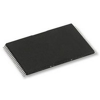
H27UAG8T2ATR-BC HYNIX SEMICONDUCTOR, H27UAG8T2ATR-BC Datasheet - Page 11

H27UAG8T2ATR-BC
Manufacturer Part Number
H27UAG8T2ATR-BC
Description
58T1891
Manufacturer
HYNIX SEMICONDUCTOR
Datasheet
1.H27UAG8T2ATR-BC.pdf
(61 pages)
Specifications of H27UAG8T2ATR-BC
Memory Type
Flash - NAND
Memory Size
16Gbit
Memory Configuration
2048M X 8
Supply Voltage Range
2.7V To 3.6V
Memory Case Style
TSOP
No. Of Pins
48
Operating Temperature Range
0°C To +70°C
Rohs Compliant
Yes
Available stocks
Company
Part Number
Manufacturer
Quantity
Price
Company:
Part Number:
H27UAG8T2ATR-BC
Manufacturer:
HYNIX
Quantity:
2 526
Company:
Part Number:
H27UAG8T2ATR-BC
Manufacturer:
SIEMENS
Quantity:
390
Company:
Part Number:
H27UAG8T2ATR-BC
Manufacturer:
HYNIX
Quantity:
4 000
Part Number:
H27UAG8T2ATR-BC
Manufacturer:
HYNIX/海力士
Quantity:
20 000
Rev 1.0 / Aug. 2010
Caution:
1.8. Mode Selection
Notes:
1. Any undefined command inputs are prohibited except for above command set.
2. Multi Plane page read, Multi Plane cache read, and Multi Plane read for copy-back must be used after Multi Plane
1. X can be VIL or VIH. H = Logic level HIGH. L = Logic level LOW.
2. WP# should be biased to CMOS high or CMOS low for stand-by mode.
3. WE# and RE# during Read Busy must be keep on high to prevent unplanned command/address/data input or to
CLE
programmed page, Multi Plane cache program, and Multi Plane copy-back program.
avert unintended data out. In this time, only Reset, Read Status, and Multi Plane Read Status can be inputted to
the device.
H
H
X
X
X
X
X
L
L
L
L
ALE
H
L
X
H
X
X
X
X
L
L
L
1)
1)
1)
CE#
H
L
L
L
L
L
L
X
X
X
X
WE#
H
H
X
X
X
X
3)
RE#
H
H
H
H
H
H
X
X
X
X
3)
0V/Vcc
WP#
16Gb (2048M x 8bit) NAND Flash
H
H
H
H
H
X
X
X
X
L
2)
Write Mode
Read Mode
Sequential Read and Data Output
During Program (Busy)
H27UAG8T2B Series
During Erase (Busy)
During Read (Busy)
Write Protect
Address Input ( 5 Cycles )
Address Input ( 5 Cycles )
Data Input
Stand-By
MODE
Command Input
Command Input
Release
11


