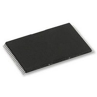
H27UAG8T2ATR-BC HYNIX SEMICONDUCTOR, H27UAG8T2ATR-BC Datasheet - Page 18

H27UAG8T2ATR-BC
Manufacturer Part Number
H27UAG8T2ATR-BC
Description
58T1891
Manufacturer
HYNIX SEMICONDUCTOR
Datasheet
1.H27UAG8T2ATR-BC.pdf
(61 pages)
Specifications of H27UAG8T2ATR-BC
Memory Type
Flash - NAND
Memory Size
16Gbit
Memory Configuration
2048M X 8
Supply Voltage Range
2.7V To 3.6V
Memory Case Style
TSOP
No. Of Pins
48
Operating Temperature Range
0°C To +70°C
Rohs Compliant
Yes
Available stocks
Company
Part Number
Manufacturer
Quantity
Price
Company:
Part Number:
H27UAG8T2ATR-BC
Manufacturer:
HYNIX
Quantity:
2 526
Company:
Part Number:
H27UAG8T2ATR-BC
Manufacturer:
SIEMENS
Quantity:
390
Company:
Part Number:
H27UAG8T2ATR-BC
Manufacturer:
HYNIX
Quantity:
4 000
Part Number:
H27UAG8T2ATR-BC
Manufacturer:
HYNIX/海力士
Quantity:
20 000
Rev 1.0 / Aug. 2010
Notes:
2.8. Status Register Coding
Notes:
I/O
1. If Reset Command (FFh) is written at Ready state, the device goes into Busy for maximum 5us.
2. Program / Erase Enable Operation: WP# high to WE# High.
3. The transition of the corresponding control pins must occur only while WE# is held low.
4. t
1.
2.
3.
4.
0
1
2
3
4
5
6
7
all other bits in the status value are valid. If cleared to zero, then the last command issued
indicates whether the last operation is complete.
Program / Erase Disable Operation: WP# Low to WE# High.
this bit is only valid when I/O5 is set to one.
second 15h command or the 10h command has been transferred in a Cache program sequence.
When Cache program is not supported, this bit is not used.
command being processed (I/O6 is cleared to zero) or an array operation in progress. When
overlapped interleaved operations or cache commands are not supported, this bit is not used.
is not yet complete and Status Register bits<5:0> are invalid value. When cache operations
are in use, then this bit indicates whether another command can be accepted, and I/O5
ADL
is the time from the WE# rising edge of final address cycle to the WE# rising edge of first data cycle.
I/O0: This bit is only valid for Program and Erase operations. During Cache Program operations,
I/O1: This bit is only valid for cache program operations. This bit is not valid until after the
I/O5: If set to one, then there is no array operation in progress. If cleared to zero, then there is a
I/O6: If set to one, then the device or interleaved address is ready for another command and
Ready / Busy
Write Protect
(Read/Program/Erase)
Program
Pass/ Fail
Device resetting time
Write protection time
Page
N/A
N/A
N/A
N/A
N/A
Ready / Busy
Write Protect
Pass/ Fail
Block
Erase
N/A
N/A
N/A
N/A
N/A
Ready / Busy
Write Protect
Read
N/A
N/A
N/A
N/A
N/A
N/A
t
t
RST
WW
Ready / Busy
Ready / Busy
Write Protect
Cache
Read
N/A
N/A
N/A
N/A
N/A
16Gb (2048M x 8bit) NAND Flash
100
Ready / Busy
Ready / Busy
Write Protect
Program
Pass/ Fail
Pass/ Fail
Cache
N/A
N/A
N/A
20/30/500
H27UAG8T2B Series
Busy : '0' Ready : '1'
Data Cache Ready /
Busy : '0' Ready : '1'
Not Protected : '1'
Pass : '0' Fail : '1'
Pass : '0' Fail : '1'
Protected : '0'
Ready / Busy
70h/ 78h
N-1 page
Coding
N page
'0'
'0'
'0'
Release
㎲
㎱
18


