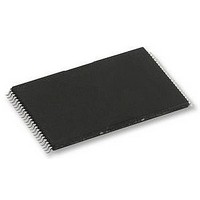
H27UAG8T2ATR-BC HYNIX SEMICONDUCTOR, H27UAG8T2ATR-BC Datasheet - Page 47

H27UAG8T2ATR-BC
Manufacturer Part Number
H27UAG8T2ATR-BC
Description
58T1891
Manufacturer
HYNIX SEMICONDUCTOR
Datasheet
1.H27UAG8T2ATR-BC.pdf
(61 pages)
Specifications of H27UAG8T2ATR-BC
Memory Type
Flash - NAND
Memory Size
16Gbit
Memory Configuration
2048M X 8
Supply Voltage Range
2.7V To 3.6V
Memory Case Style
TSOP
No. Of Pins
48
Operating Temperature Range
0°C To +70°C
Rohs Compliant
Yes
Available stocks
Company
Part Number
Manufacturer
Quantity
Price
Company:
Part Number:
H27UAG8T2ATR-BC
Manufacturer:
HYNIX
Quantity:
2 526
Company:
Part Number:
H27UAG8T2ATR-BC
Manufacturer:
SIEMENS
Quantity:
390
Company:
Part Number:
H27UAG8T2ATR-BC
Manufacturer:
HYNIX
Quantity:
4 000
Part Number:
H27UAG8T2ATR-BC
Manufacturer:
HYNIX/海力士
Quantity:
20 000
Rev 1.0 / Aug. 2010
with destination page address. Actual programming operation begins after Program Confirm command (10h) is issued.
Once the program process starts, the Read Status Register command (70h) may be entered to read the status register.
The system controller can detect the completion of a program cycle by monitoring the R/B# output, or the Status bit
(I/O 6) of the Status Register. When the Copy-Back Program is complete, the Write Status Bit (I/O 0) may be checked.
The command register remains in Read Status command mode until another valid command is written to the com-
mand register. During copy-back program, data modification is possible using random data input command (85h) as
shown in Figure 45.
4.12. Multi Plane Copy-Back Program
Multi plane Copy-Back Program is an extension of Copy-Back Program, for a single plane with 8,640 byte page regis-
ters. Since the device is equipped with two memory planes, activating the two sets of 8,640-byte page registers
enables a simultaneous programming of two pages. Figure 46 and Figure 47 show command sequence for the Multi
Plane copy-back operation. First case, Figure 46, shows random data input of two planes that started right after finish-
ing random data output of previous two planes. Second case, Figure 47, shows the random data input of each plane
which started right after finishing the random data output of each Plane.
■ Figure 45. Copyback program
R/B#
R/B#
I/Ox
I/Ox
A
85h
00h
Target Address
Address
(5 cycle)
Source Address
(5 cycle)
Address
Data
35h
85h
address 1,2
Address
(2 cycle)
Column
t
R
Data
16Gb (2048M x 8bit) NAND Flash
10h
Data output
t
PROG
H27UAG8T2B Series
A
70h
Status
Release
47


