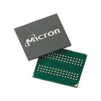
MT48H8M32LFB5-75 IT:H Micron Technology Inc, MT48H8M32LFB5-75 IT:H Datasheet - Page 9

MT48H8M32LFB5-75 IT:H
Manufacturer Part Number
MT48H8M32LFB5-75 IT:H
Description
DRAM Chip Mobile SDRAM 256M-Bit 8Mx32 1.8V 90-Pin VFBGA Tray
Manufacturer
Micron Technology Inc
Type
Mobile SDRAMr
Specifications of MT48H8M32LFB5-75 IT:H
Density
256 Mb
Maximum Clock Rate
133 MHz
Package
90VFBGA
Address Bus Width
14 Bit
Operating Supply Voltage
1.8 V
Maximum Random Access Time
8|6 ns
Operating Temperature
-40 to 85 °C
Format - Memory
RAM
Memory Type
Mobile SDRAM
Memory Size
256M (8Mx32)
Speed
133MHz
Interface
Parallel
Voltage - Supply
1.7 V ~ 1.95 V
Package / Case
90-VFBGA
Organization
8Mx32
Address Bus
14b
Access Time (max)
8/6ns
Operating Supply Voltage (typ)
1.8V
Package Type
VFBGA
Operating Temp Range
-40C to 85C
Operating Supply Voltage (max)
1.95V
Operating Supply Voltage (min)
1.7V
Supply Current
100mA
Pin Count
90
Mounting
Surface Mount
Operating Temperature Classification
Industrial
Lead Free Status / RoHS Status
Lead free / RoHS Compliant
Functional Block Diagram
Figure 2: Functional Block Diagram
PDF: 09005aef834c13d2
256mb_mobile_sdram_y36n.pdf - Rev. I 11/09 EN
BA0, BA1
Address
CAS#
RAS#
WE#
CKE
CLK
CS#
Address
register
Mode register
EXT mode
register
Control
logic
Refresh
counter
2
address
2
MUX
Row
Column/
counter/
address
control
Bank
latch
logic
256Mb: 16 Meg x 16, 8 Meg x 32 Mobile SDRAM
decoder
address
Bank0
latch
row
and
9
DQM mask logic
Sense amplifiers
read data latch
write drivers
I/O gating
decoder
memory
Column
Micron Technology, Inc. reserves the right to change products or specifications without notice.
Bank0
Bank1
array
Bank2
Bank3
Functional Block Diagram
BA1
n
n
0
0
1
1
©2008 Micron Technology, Inc. All rights reserved.
register
register
output
BA0
input
Data
Data
0
1
0
1
Bank
0
1
2
3
n
DQM
DQ


