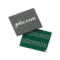
MT48H8M32LFB5-75 IT:H Micron Technology Inc, MT48H8M32LFB5-75 IT:H Datasheet - Page 49

MT48H8M32LFB5-75 IT:H
Manufacturer Part Number
MT48H8M32LFB5-75 IT:H
Description
DRAM Chip Mobile SDRAM 256M-Bit 8Mx32 1.8V 90-Pin VFBGA Tray
Manufacturer
Micron Technology Inc
Type
Mobile SDRAMr
Specifications of MT48H8M32LFB5-75 IT:H
Density
256 Mb
Maximum Clock Rate
133 MHz
Package
90VFBGA
Address Bus Width
14 Bit
Operating Supply Voltage
1.8 V
Maximum Random Access Time
8|6 ns
Operating Temperature
-40 to 85 °C
Format - Memory
RAM
Memory Type
Mobile SDRAM
Memory Size
256M (8Mx32)
Speed
133MHz
Interface
Parallel
Voltage - Supply
1.7 V ~ 1.95 V
Package / Case
90-VFBGA
Organization
8Mx32
Address Bus
14b
Access Time (max)
8/6ns
Operating Supply Voltage (typ)
1.8V
Package Type
VFBGA
Operating Temp Range
-40C to 85C
Operating Supply Voltage (max)
1.95V
Operating Supply Voltage (min)
1.7V
Supply Current
100mA
Pin Count
90
Mounting
Surface Mount
Operating Temperature Classification
Industrial
Lead Free Status / RoHS Status
Lead free / RoHS Compliant
Figure 18: Random READ Accesses
PDF: 09005aef834c13d2
256mb_mobile_sdram_y36n.pdf - Rev. I 11/09 EN
Note:
Command
Command
Data from any READ burst can be truncated with a subsequent WRITE command, and
data from a fixed-length READ burst can be followed immediately by data from a
WRITE command (subject to bus turnaround limitations). The WRITE burst can be initi-
ated on the clock edge immediately following the last (or last desired) data element
from the READ burst, provided that I/O contention can be avoided. In a given system
design, there is a possibility that the device driving the input data will go Low-Z before
the DQ go High-Z. In this case, at least a single-cycle delay should occur between the
last read data and the WRITE command.
The DQM input is used to avoid I/O contention, as shown in Figure 19 (page 50) and
Figure 20 (page 51). The DQM signal must be asserted (HIGH) at least two clocks prior
to the WRITE command (DQM latency is two clocks for output buffers) to suppress data-
out from the READ. After the WRITE command is registered, the DQ will go to High-Z
(or remain High-Z), regardless of the state of the DQM signal, provided the DQM was
active on the clock just prior to the WRITE command that truncated the READ com-
mand. If not, the second WRITE will be an invalid WRITE. For example, if DQM was
LOW during T4, then the WRITEs at T5 and T7 would be valid, and the WRITE at T6
would be invalid.
Address
Address
1. Each READ command can be issued to any bank. DQM is LOW.
CLK
CLK
DQ
DQ
T0
T0
READ
Bank,
READ
Bank,
Col n
Col n
CL = 2
T1
T1
READ
READ
Bank,
Bank,
Col a
Col a
256Mb: 16 Meg x 16, 8 Meg x 32 Mobile SDRAM
CL = 3
49
T2
T2
Bank,
Bank,
READ
READ
Col x
Col x
D
OUT
T3
T3
Micron Technology, Inc. reserves the right to change products or specifications without notice.
READ
Bank,
Col m
READ
Bank,
Col m
D
D
OUT
OUT
T4
T4
NOP
NOP
D
D
OUT
OUT
T5
T5
NOP
NOP
D
D
OUT
OUT
©2008 Micron Technology, Inc. All rights reserved.
T6
Don’t Care
READ Operation
NOP
D
OUT


