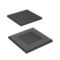
HD6417712BPV Renesas Electronics America, HD6417712BPV Datasheet - Page 476

HD6417712BPV
Manufacturer Part Number
HD6417712BPV
Description
MPU 1.5/3.3V 0K PB-FREE 256-BGA
Manufacturer
Renesas Electronics America
Series
SuperH® SH Ethernetr
Datasheet
1.HD6417712BPV.pdf
(980 pages)
Specifications of HD6417712BPV
Core Processor
SH-3 DSP
Core Size
32-Bit
Speed
200MHz
Connectivity
EBI/EMI, Ethernet, FIFO, SCI, SIO
Peripherals
DMA, POR, WDT
Number Of I /o
24
Program Memory Type
ROMless
Ram Size
16K x 8
Voltage - Supply (vcc/vdd)
1.4 V ~ 1.6 V
Oscillator Type
External
Operating Temperature
-20°C ~ 75°C
Package / Case
256-BGA
Lead Free Status / RoHS Status
Lead free / RoHS Compliant
Eeprom Size
-
Program Memory Size
-
Data Converters
-
Available stocks
Company
Part Number
Manufacturer
Quantity
Price
Company:
Part Number:
HD6417712BPV
Manufacturer:
Renesas Electronics America
Quantity:
10 000
- Current page: 476 of 980
- Download datasheet (6Mb)
Section 12 Bus State Controller (BSC)
Relationship between Refresh Requests and Bus Cycles: If a refresh request occurs during bus
cycle execution, the refresh cycle must wait for the bus cycle to be completed. If a refresh request
occurs while the bus is released by the bus arbitration function, the refresh will not be executed
until the bus mastership is acquired. This LSI supports requests by the REFOUT pin for the bus
mastership while waiting for the refresh request. The REFOUT pin is asserted low until the bus
mastership is acquired.
If a new refresh request occurs while waiting for the previous refresh request, the previous refresh
request is deleted. To refresh correctly, a bus cycle longer than the refresh interval or the bus
mastership occupation must be prevented from occurring. If a bus mastership is requested during
self-refresh, the bus will not be released until the self-refresh is completed.
Low-Frequency Mode: When the SLOW bit in SDCR is set to 1, output of commands, addresses,
and write data, and fetch of read data are performed at a timing suitable for operating SDRAM at a
low frequency.
Rev. 1.00 Dec. 27, 2005 Page 432 of 932
REJ09B0269-0100
A12/A11*
D31 to D0
A25 to A0
DACKn*
DQMxx
RD/WR
Notes: 1. Address pin to be connected to the A10 pin of SDRAM.
CKIO
CKE
RAS
CAS
CSn
BS
1
2
2. The waveform for DACKn is when active low is specified.
Tp
Tpw
Figure 12.26 Self-Refresh Timing
Trr
Hi-z
Trc
Trc
Trc
Trc
Trc
Related parts for HD6417712BPV
Image
Part Number
Description
Manufacturer
Datasheet
Request
R

Part Number:
Description:
KIT STARTER FOR M16C/29
Manufacturer:
Renesas Electronics America
Datasheet:

Part Number:
Description:
KIT STARTER FOR R8C/2D
Manufacturer:
Renesas Electronics America
Datasheet:

Part Number:
Description:
R0K33062P STARTER KIT
Manufacturer:
Renesas Electronics America
Datasheet:

Part Number:
Description:
KIT STARTER FOR R8C/23 E8A
Manufacturer:
Renesas Electronics America
Datasheet:

Part Number:
Description:
KIT STARTER FOR R8C/25
Manufacturer:
Renesas Electronics America
Datasheet:

Part Number:
Description:
KIT STARTER H8S2456 SHARPE DSPLY
Manufacturer:
Renesas Electronics America
Datasheet:

Part Number:
Description:
KIT STARTER FOR R8C38C
Manufacturer:
Renesas Electronics America
Datasheet:

Part Number:
Description:
KIT STARTER FOR R8C35C
Manufacturer:
Renesas Electronics America
Datasheet:

Part Number:
Description:
KIT STARTER FOR R8CL3AC+LCD APPS
Manufacturer:
Renesas Electronics America
Datasheet:

Part Number:
Description:
KIT STARTER FOR RX610
Manufacturer:
Renesas Electronics America
Datasheet:

Part Number:
Description:
KIT STARTER FOR R32C/118
Manufacturer:
Renesas Electronics America
Datasheet:

Part Number:
Description:
KIT DEV RSK-R8C/26-29
Manufacturer:
Renesas Electronics America
Datasheet:

Part Number:
Description:
KIT STARTER FOR SH7124
Manufacturer:
Renesas Electronics America
Datasheet:

Part Number:
Description:
KIT STARTER FOR H8SX/1622
Manufacturer:
Renesas Electronics America
Datasheet:

Part Number:
Description:
KIT DEV FOR SH7203
Manufacturer:
Renesas Electronics America
Datasheet:


