DV164136 Microchip Technology, DV164136 Datasheet - Page 71

DV164136
Manufacturer Part Number
DV164136
Description
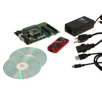
DEVELOPMENT KIT FOR PIC18
Manufacturer
Microchip Technology
Series
PIC®r
Type
MCUr
Datasheets
1.DM183032.pdf
(38 pages)
2.DV164136.pdf
(448 pages)
3.DV164136.pdf
(6 pages)
4.DV164136.pdf
(446 pages)
5.DV164136.pdf
(4 pages)
6.DV164136.pdf
(18 pages)
Specifications of DV164136
Contents
Board, Cables, CDs, PICkit™ 3 Programmer, Power Supply
Processor To Be Evaluated
PIC18F8722, PIC18F87J11
Interface Type
RS-232, USB
Operating Supply Voltage
3.3 V, 5 V
Silicon Manufacturer
Microchip
Core Architecture
PIC
Core Sub-architecture
PIC18
Silicon Core Number
PIC18F
Silicon Family Name
PIC18F8xxx
Kit Contents
PIC18 Exp Brd PICkit 3 Cable CD PSU
Lead Free Status / RoHS Status
Lead free / RoHS Compliant
For Use With/related Products
PIC18F8722, PIC18F87J11
Lead Free Status / Rohs Status
Lead free / RoHS Compliant
Available stocks
Company
Part Number
Manufacturer
Quantity
Price
Company:
Part Number:
DV164136
Manufacturer:
MICROCHIP
Quantity:
12 000
- DM183032 PDF datasheet
- DV164136 PDF datasheet #2
- DV164136 PDF datasheet #3
- DV164136 PDF datasheet #4
- DV164136 PDF datasheet #5
- DV164136 PDF datasheet #6
- Current page: 71 of 446
- Download datasheet (7Mb)
5.1.5.2
A better method of storing data in program memory
allows two bytes of data to be stored in each instruction
location.
Look-up table data may be stored two bytes per pro-
gram word by using table reads and writes. The Table
Pointer (TBLPTR) register specifies the byte address
and the Table Latch (TABLAT) register contains the
data that is read from or written to program memory.
Data is transferred to or from program memory one
byte at a time.
Table read and table write operations are discussed
further in Section 6.1 “Table Reads and Table
Writes”.
5.2
5.2.1
The microcontroller clock input, whether from an internal
or external source, is internally divided by four to gener-
ate four non-overlapping quadrature clocks (Q1, Q2, Q3
and Q4). Internally, the program counter is incremented
on every Q1; the instruction is fetched from the program
FIGURE 5-4:
EXAMPLE 5-3:
© 2008 Microchip Technology Inc.
1. MOVLW 55h
2. MOVWF PORTB
3. BRA
4. BSF
5. Instruction @ address SUB_1
All instructions are single cycle, except for any program branches. These take two cycles since the fetch instruction
is “flushed” from the pipeline while the new instruction is being fetched and then executed.
OSC2/CLKO
(RC mode)
PIC18 Instruction Cycle
SUB_1
CLOCKING SCHEME
PORTA, BIT3 (Forced NOP)
OSC1
Table Reads and Table Writes
PC
Q1
Q2
Q3
Q4
CLOCK/INSTRUCTION CYCLE
Q1
INSTRUCTION PIPELINE FLOW
Execute INST (PC – 2)
Fetch INST (PC)
Q2
Fetch 1
T
PC
CY
0
Q3
Q4
Execute 1
Fetch 2
T
CY
1
Q1
Fetch INST (PC + 2)
Execute INST (PC)
Execute 2
Q2
Fetch 3
PC + 2
T
CY
2
memory and latched into the instruction register during
Q4. The instruction is decoded and executed during the
following Q1 through Q4. The clocks and instruction
execution flow are shown in Figure 5-4.
5.2.2
An “Instruction Cycle” consists of four Q cycles: Q1
through Q4. The instruction fetch and execute are
pipelined in such a manner that a fetch takes one
instruction cycle, while the decode and execute take
another instruction cycle. However, due to the pipe-
lining, each instruction effectively executes in one
cycle. If an instruction causes the program counter to
change (e.g., GOTO), then two cycles are required to
complete the instruction (Example 5-3).
A fetch cycle begins with the program counter
incrementing in Q1.
In the execution cycle, the fetched instruction is latched
into the Instruction Register (IR) in cycle Q1. This
instruction is then decoded and executed during the
Q2, Q3 and Q4 cycles. Data memory is read during Q2
(operand read) and written during Q4 (destination
write).
Q3
PIC18F8722 FAMILY
Q4
Execute 3
Fetch 4
T
CY
INSTRUCTION FLOW/PIPELINING
3
Q1
Execute INST (PC + 2)
Fetch INST (PC + 4)
Fetch SUB_1 Execute SUB_1
Flush (NOP)
Q2
T
PC + 4
CY
4
Q3
Q4
DS39646C-page 69
T
CY
Internal
Phase
Clock
5
Related parts for DV164136
Image
Part Number
Description
Manufacturer
Datasheet
Request
R

Part Number:
Description:
Manufacturer:
Microchip Technology Inc.
Datasheet:

Part Number:
Description:
Manufacturer:
Microchip Technology Inc.
Datasheet:

Part Number:
Description:
Manufacturer:
Microchip Technology Inc.
Datasheet:

Part Number:
Description:
Manufacturer:
Microchip Technology Inc.
Datasheet:

Part Number:
Description:
Manufacturer:
Microchip Technology Inc.
Datasheet:

Part Number:
Description:
Manufacturer:
Microchip Technology Inc.
Datasheet:

Part Number:
Description:
Manufacturer:
Microchip Technology Inc.
Datasheet:

Part Number:
Description:
Manufacturer:
Microchip Technology Inc.
Datasheet:


