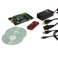
DV164136 Microchip Technology, DV164136 Datasheet - Page 102

DV164136
Manufacturer Part Number
DV164136
Description
DEVELOPMENT KIT FOR PIC18
Manufacturer
Microchip Technology
Series
PIC®r
Type
MCUr
Datasheets
1.DM183032.pdf
(38 pages)
2.DV164136.pdf
(448 pages)
3.DV164136.pdf
(6 pages)
4.DV164136.pdf
(446 pages)
5.DV164136.pdf
(4 pages)
6.DV164136.pdf
(18 pages)
Specifications of DV164136
Contents
Board, Cables, CDs, PICkit™ 3 Programmer, Power Supply
Processor To Be Evaluated
PIC18F8722, PIC18F87J11
Interface Type
RS-232, USB
Operating Supply Voltage
3.3 V, 5 V
Silicon Manufacturer
Microchip
Core Architecture
PIC
Core Sub-architecture
PIC18
Silicon Core Number
PIC18F
Silicon Family Name
PIC18F8xxx
Kit Contents
PIC18 Exp Brd PICkit 3 Cable CD PSU
Lead Free Status / RoHS Status
Lead free / RoHS Compliant
For Use With/related Products
PIC18F8722, PIC18F87J11
Lead Free Status / Rohs Status
Lead free / RoHS Compliant
Available stocks
Company
Part Number
Manufacturer
Quantity
Price
Company:
Part Number:
DV164136
Manufacturer:
MICROCHIP
Quantity:
12 000
- DM183032 PDF datasheet
- DV164136 PDF datasheet #2
- DV164136 PDF datasheet #3
- DV164136 PDF datasheet #4
- DV164136 PDF datasheet #5
- DV164136 PDF datasheet #6
- Current page: 102 of 446
- Download datasheet (7Mb)
PIC18F8722 FAMILY
7.4
PIC18F8527/8622/8627/8722 devices are capable of
operating in any one of four program memory modes,
using combinations of on-chip and external program
memory. The functions of the multiplexed port pins
depends on the program memory mode selected, as
well as the setting of the EBDIS bit.
In Microcontroller Mode, the bus is not active and the
pins have their port functions only. Writes to the
MEMCOM register are not permitted. The Reset value
of EBDIS (‘0’) is ignored and EMB pins behave as I/O
ports.
In Microprocessor Mode, the external bus is always
active and the port pins have only the external bus
function. The value of EBDIS is ignored.
In Microprocessor with Boot Block or Extended
Microcontroller Mode, the external program memory
bus shares I/O port functions on the pins. When the
device is fetching or doing table read/table write opera-
tions on the external program memory space, the pins
will have the external bus function. If the device is
fetching and accessing internal program memory loca-
tions only, the EBDIS control bit will change the pins
from external memory to I/O port functions. When
EBDIS = 0, the pins function as the external bus. When
EBDIS = 1, the pins function as I/O ports.
If the device fetches or accesses external memory
while EBDIS = 1, the pins will switch from I/O to exter-
nal bus. If the EBDIS bit is set by a program executing
from external memory, the action of setting the bit will
be delayed until the program branches into the internal
memory. At that time, the pins will change from external
bus to I/O ports.
If the device is executing out of internal memory when
EBDIS = 0, the memory bus address/data and control
pins will not be active. They will go to a state where the
active address/data pins are tri-state; the CE, OE,
WRH, WRL, UB and LB signals are ‘1’; and ALE and
BA0 are ‘0’. Note that only those pins associated with
the current address width are forced to tri-state; the
other pins continue to function as I/O. In the case of
16-bit address width, for example, only AD<15:0>
(PORTD and PORTE) are affected; A<19:16>
(PORTH<3:0>) continue to function as I/O.
In all external memory modes, the bus takes priority
over any other peripherals that may share pins with it.
This includes the Parallel Slave Port and serial commu-
nications modules which would otherwise take priority
over the I/O port.
DS39646C-page 100
Program Memory Modes and the
External Memory Bus
7.5
In 16-Bit Data Width mode, the External Memory Bus
can be connected to external memories in three
different configurations:
• 16-bit Byte Write
• 16-bit Word Write
• 16-bit Byte Select
The configuration to be used is determined by the
WM1:WM0
(MEMCON<1:0>). These three different configurations
allow the designer maximum flexibility in using both
8-bit and 16-bit devices with 16-bit data.
For all 16-bit modes, the Address Latch Enable (ALE)
pin indicates that the address bits AD<15:0> are
available on the external memory interface bus.
Following the address latch, the Output Enable signal
(OE) will enable both bytes of program memory at once
to form a 16-bit instruction word. The Chip Enable
signal (CE) is active at any time that the microcontroller
accesses external memory, whether reading or writing;
it is inactive (asserted high) whenever the device is in
Sleep mode.
In Byte Select mode, JEDEC standard Flash memories
will require BA0 for the byte address line and one I/O
line to select between Byte and Word mode. The other
16-bit modes do not need BA0. JEDEC standard static
RAM memories will use the UB or LB signals for byte
selection.
16-Bit Data Width Modes
bits
in
© 2008 Microchip Technology Inc.
the
MEMCON
register
Related parts for DV164136
Image
Part Number
Description
Manufacturer
Datasheet
Request
R

Part Number:
Description:
Manufacturer:
Microchip Technology Inc.
Datasheet:

Part Number:
Description:
Manufacturer:
Microchip Technology Inc.
Datasheet:

Part Number:
Description:
Manufacturer:
Microchip Technology Inc.
Datasheet:

Part Number:
Description:
Manufacturer:
Microchip Technology Inc.
Datasheet:

Part Number:
Description:
Manufacturer:
Microchip Technology Inc.
Datasheet:

Part Number:
Description:
Manufacturer:
Microchip Technology Inc.
Datasheet:

Part Number:
Description:
Manufacturer:
Microchip Technology Inc.
Datasheet:

Part Number:
Description:
Manufacturer:
Microchip Technology Inc.
Datasheet:


